LTC3101
APPLICATIONS INFORMATION
buck converter is going to be utilized at duty cycles over
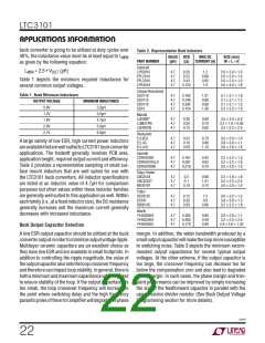
Table 2. Representative Buck Inductors
40%, the inductance value must be at least equal to L
VALUE DCR
MAX DC
CURRENT (A)
SIZE (mm)
W × L × H
MIN
PART NUMBER
(ꢀH)
(Ω)
as given by the following equation:
Coilcraft
LPS3015
EPL2014
EPL2010
LPS4018
L
= 2.5 • V
(μH)
4.7
4.7
4.7
4.7
0.20
0.23
1.2
0.88
0.65
1.9
3.0 × 3.0 × 1.5
2.0 × 2.0 × 1.4
2.0 × 2.0 × 1.0
4.0 × 4.0 × 1.8
MIN
OUT
Table 1 depicts the minimum required inductance for
several common output voltages.
0.43
0.125
Cooper-Bussmann
SD3118
Table 1. Buck Minimum Inductance
4.7
4.7
4.7
4.7
0.162
0.246
0.285
0.154
1.31
0.80
0.68
1.08
3.1 × 3.1 × 1.8
3.1 × 3.1 × 1.2
3.1 × 3.1 × 1.0
5.2 × 5.2 × 1.0
SD3112
OUTPUT VOLTAGE
MINIMUM INDUCTANCE
SD3110
SD10
0.8V
1.2V
1.8V
2.0V
2.7V
2.0ꢀH
3.0ꢀH
4.7ꢀH
5.0ꢀH
6.8ꢀH
Murata
LQH3NP
LQM31PN
LQH32CN
4.7
4.7
4.7
0.26
0.30
0.15
0.80
0.70
0.65
3.0 × 3.0 × 0.9
3.2 × 1.6 × 0.85
3.2 × 2.5 × 2.0
Panasonic
ELLVEG
ELL4G
4.7
4.7
4.7
0.24
0.16
0.09
0.70
0.86
1.10
3.0 × 3.0 × 1.0
3.8 × 3.8 × 1.1
3.8 × 3.8 × 1.8
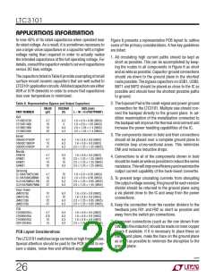
A large variety of low ESR, high current power inductors
areavailablethatarewellsuitedtoLTC3101buckconverter
applications. The tradeoff generally involves PCB area,
application height, required output current and efficiency.
Table 2 provides a representative sampling of small sur-
face mount inductors that are well suited for use with
the LTC3101 buck converters. All inductor specifications
are listed at an inductor value of 4.7μH for comparison
purposes but other values within these inductor families
are generally well suited to this application as well. Within
eachfamily(i.e.,atafixedinductorsize),theDCresistance
generally increases and the maximum current generally
decreases with increased inductance.
ELL4LG
Sumida
CDRH2D09
CDRH3D16/LD
CDRH2D09B
4.7
4.7
4.7
0.167
0.081
0.218
0.42
0.62
0.70
3.2 × 3.2 × 1.0
3.2 × 3.2 × 1.8
3.0 × 2.8 × 1.0
Taiyo-Yuden
CBC2518
CBC3225T
NR3010T
4.7
4.7
4.7
0.2
0.1
0.19
0.68
1.01
0.75
2.5 × 1.8 × 1.8
3.2 × 2.5 × 2.5
3.0 × 3.0 × 1.0
TOKO
DE2812C
D310F
4.7
4.7
4.7
0.13
0.26
0.09
1.2
0.9
3.0 × 3.2 × 1.2
3.8 × 3.8 × 1.0
3.2 × 3.2 × 1.8
DB3015C
0.86
Wurth
744028004
744032004
744029003
4.7
4.7
4.7
0.265
0.280
0.170
0.90
0.49
0.80
2.8 × 2.8 × 1.1
3.2 × 2.5 × 2.0
2.8 × 2.8 × 1.35
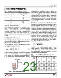
Buck Output Capacitor Selection
margin. In addition, the wider bandwidth produced by a
smalloutputcapacitorwillmaketheloopmoresusceptible
to switching noise. Table 3 depicts the minimum recom-
mended output capacitance for several typical output
voltages. At the other extreme, if the output capacitor is
too large, the crossover frequency can decrease too far
below the compensation zero and also lead to degraded
phase margin. In such cases, the phase margin and tran-
sient performance can be improved by simply increasing
the size of the feedforward capacitor in parallel with the
upper resistor divider resistor. (See Buck Output Voltage
Programming section for more details).
A low ESR output capacitor should be utilized at the buck
converteroutputinordertominimizeoutputvoltageripple.
Multilayer ceramic capacitors are an excellent choice as
they have low ESR and are available in small footprints. In
addition to controlling the ripple magnitude, the value of
theoutputcapacitoralsosetstheloopcrossoverfrequency
and therefore can impact loop stability. In general, there is
bothaminimumandmaximumcapacitancevaluerequired
to ensure stability of the loop. If the output capacitance is
too small, the loop crossover frequency will increase to
the point where switching delay and the high frequency
parasiticpolesoftheerroramplifierwilldegradethephase
3101f
22

 Linear [ Linear ]