LTC3101
APPLICATIONS INFORMATION
to lose 45% of its rated capacitance when operated near
its rated voltage. As a result, it is sometimes necessary to
use a larger value capacitance or a capacitor with a higher
voltage rating than required in order to actually realize
the intended capacitance at the full operating voltage. For
details,consultthecapacitorvendor’scurveofcapacitance
versus DC bias voltage.
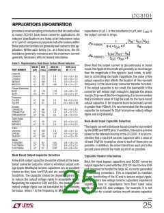
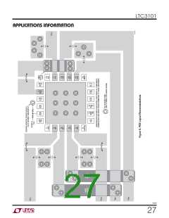
Figure 6 presents a representative PCB layout to outline
some of the primary considerations. A few key guidelines
are listed:
1. All circulating high current paths should be kept as
short as possible. This can be accomplished by keep-
ing the routes to all components in Figure 6 as short
and as wide as possible. Capacitor ground connections
should via down to the ground plane in the shortest
route possible. The bypass capacitors on USB1, USB2,
BAT1 and BAT2 should be placed as close to the IC as
possible and should have the shortest possible paths
to ground.
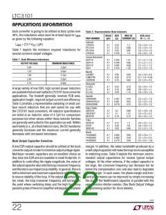
ThecapacitorslistedinTable6provideasamplingofsmall
surface mount ceramic capacitors that are well suited to
LTC3101applicationcircuits.Alllistedcapacitorsareeither
X5R or X7R dielectric in order to ensure that capacitance
loss over temperature is minimized.
Table 6. Representative Bypass and Output Capacitors
2. The Exposed Pad is the small-signal and power ground
connection for the LTC3101. Multiple vias should con-
nect the backpad directly to the ground plane. In ad-
dition maximization of the metallization connected to
the backpad will improve the thermal environment and
increase the power handling capabilities of the IC.
VALUE
(ꢀF)
VOLTAGE
(V)
SIZE (mm)
L × W × H (FOOTPRINT)
PART NUMBER
AVX
12106D475K
12104D106K
12106D106K
12106D226K
4.7
10
10
22
6.3
4
6.3
6.3
1.6 × 0.8 × 0.86 (0603)
1.6 × 0.8 × 1.02 (0603)
2.0 × 1.25 × 1.4 (0805)
2.0 × 1.25 × 1.4 (0805)
3. The components shown in bold and their connections
should all be placed over a complete ground plane to
minimize loop cross-sectional areas. This minimizes
EMI and reduces inductive drops.
Kemet
C0603C475K9P
C0603C106K9P
C0805C476K9P
4.7
10
47
6.3
6.3
6.3
1.6 × 0.8 × 0.8 (0603)
1.6 × 0.8 × 0.8 (0603)
2.0 × 1.25 × 1.25 (0805)
Murata
GRM18
GRM21
GRM21
GRM21
4.7
4.7
10
6.3
10
1.6 × 0.8 × 0.8 (0603)
2.0 × 1.25 × 1.25 (0805)
2.0 × 1.25 × 1.25 (0805)
2.0 × 1.25 × 1.25 (0805)
4. Connections to all of the components shown in bold
shouldbemadeaswideaspossibletoreducetheseries
resistance.Thiswillimproveefficiencyandmaximizethe
output current capability of the buck-boost converter.
10
22
6.3
Samsung
CL10A475KP5LNN
CL10A106KQ8NNN
CL21A226MQCLRN
CL21A476MQYNNN
4.7
10
22
47
10
6.3
6.3
6.3
1.6 × 0.8 × 0.55 (0603)
1.6 × 0.8 × 0.90 (0603)
2.0 × 1.25 × 0.95 (0805)
2.0 × 1.25 × 1.45 (0805)
5. To prevent large circulating currents from disrupting
theoutputvoltagesensing, thegroundforeachresistor
divider should be returned to the ground plane using
a via placed close to the IC and away from the power
connections.
Taiyo Yuden
JMK107BJ
LMK107BJ
JMK212BJ
JMK212BJ
10
4.7
22
47
6.3
10
6.3
6.3
1.6 × 0.8 × 0.8 (0603)
1.6 × 0.8 × 0.8 (0603)
2.0 × 1.25 × 0.85 (0805)
2.0 × 1.25 × 0.85 (0805)
6. Keep the connection from the resistor dividers to the
feedback pins FB1 and FB2 as short as possible and
away from the switch pin connections.
TDK
C1608X5ROJ
C1608X5R0J
C1608X5R0J
C2012X5R0J
4.7
6.8
10
6.3
6.3
6.3
6.3
1.6 × 0.8 × 0.8 (0603)
1.6 × 0.8 × 0.8 (0603)
1.6 × 0.8 × 0.8 (0603)
2.0 × 1.25 × 0.85 (0805)
7. Crossover connections (such as the one shown from
SW3A to the inductor) should be made on inner copper
layers if available. If it is necessary to place these on
the ground plane, make the trace on the ground plane
as short as possible to minimize the disruption to the
ground plane.
15
PCB Layout Considerations
The LTC3101 switches large currents at high frequencies.
Special attention should be paid to the PCB layout to en-
sure a stable, noise-free and efficient application circuit.
3101f
26

 Linear [ Linear ]