LTC3101
APPLICATIONS INFORMATION
capacitance of the feedback pin produce a parasitic pole
that can reduce the loop phase margin if it becomes too
low in frequency. For these reasons, it is recommended
that the resistance of R1 in parallel with R2 be kept under
300k. A reasonable compromise between noise immu-
nity and quiescent current is provided by choosing R2 =
221k. The required value for R1 can then be calculated
via Equation 1.
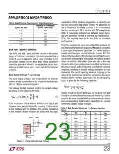
Table 3. Buck Minimum Recommended Output Capacitance
MINIMUM RECOMMENDED
OUTPUT VOLTAGE
OUTPUT CAPACITANCE
0.6V
0.8V
1.2V
1.8V
2.7V
3.3V
22ꢀF
22ꢀF
10ꢀF
10ꢀF
4.7ꢀF
4.7ꢀF
To further increase the noise immunity of the feedback pin
and improve the transient response of the buck converter,
Buck Input Capacitor Selection
a small value feedforward capacitor, C , can be added in
FF
parallel with the upper feedback divider resistor, R2. This
reducestheimpedanceofthefeedbackpinathighfrequen-
cies thereby increasing its immunity from picking up stray
noise. In addition, this adds a pole-zero pair to the loop
dynamicswhichgeneratesaphaseboostthatcanimprove
the phase margin and increase the speed of the transient
response, resulting in smaller voltage deviation on load
transients. The zero frequency depends not only on the
value of the feedforward capacitor, but also on the upper
resistor divider resistor. Specifically, the zero frequency,
The BAT1 and USB1 pins provides current to the power
stages of both buck converters. It is recommended that a
low ESR ceramic capacitor with a value of at least 4.7μF
be used to bypass each of these pins. These capacitors
should be placed as close to the respective pin as pos-
sible and should have a short return path to the backpad
of the IC.
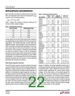
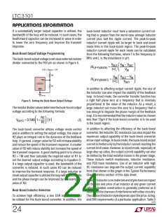
Buck Output Voltage Programming
The buck output voltages are programmed via external
resistor dividers connected to the respective feedback pin
(FB1 or FB2) as shown in Figure 4.
f
, is given by the following equation:
ZERO
1
fZERO
=
2 • π •R2 •CFF
The resistor divider resistors control the output voltage
according to the following formula:
Ideally, the phase boost generated by the pole-zero pair
shouldbecenteredattheloopcrossoverfrequency.Table 4
providestherecommendedfeedbackdividerresistorvalues
and corresponding feedforward capacitors for several
commonly utilized output voltages.
⎛
⎞
R2
R1
(1)
VOUT1,2 = 0.596 1+
V
( )
⎜
⎝
⎟
⎠
If the impedance of the resistor divider is too high it will
increase noise sensitivity due to coupling of stray noise
to the feedback pin. In addition, the parallel resistance
of the resistor divider resistors in series with the input
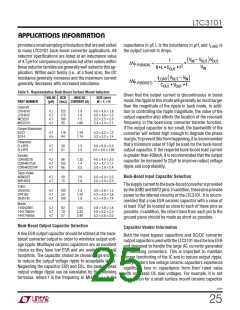
Table 4. Buck Resistor Divider and Feedforward Capacitor
Values
V
R1
R2
C
C
OUT
OUT
FF
0.6V
0.8V
1.0V
1.2V
1.5V
1.8V
2.0V
2.7V
3.3V
–
0
–
22μF
22μF
22μF
10μF
10μF
10μF
10μF
4.7μF
4.7μF
V
≥ 0.600V
OUT1,2
649k
324k
221k
147k
110k
86.6k
56.2k
48.7k
221k
221k
221k
221k
221k
205k
200k
221k
18pF
18pF
18pF
18pF
18pF
18pF
18pF
18pF
R2
C
FF
FB1,2
LTC3101
R1
GND
3101 F04
Figure 4. Setting the Buck Output Voltages
3101f
23

 Linear [ Linear ]