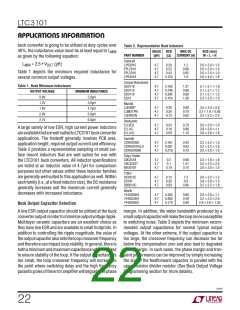
LTC3101
OPERATION
switch A remains on for a larger portion of the switching
cycle. When the duty cycle reaches approximately 85%,
the switch pair AC begins turning on for a small fraction
of the switching period. As the input voltage decreases
further, the AC switch pair remains on for longer durations
andthedurationoftheBDphasedecreasesproportionally.
As the input voltage drops below the output voltage, the
AC phase will eventually increase to the point that there is
no longer any BD phase. At this point, switch A remains on
continuously while switch pair CD is pulse width modu-
lated to obtain the desired output voltage. At this point,
the converter is operating solely in boost mode.
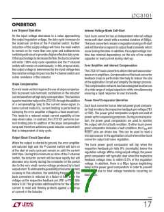
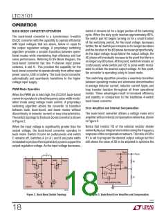
BUCK-BOOST CONVERTER OPERATION
The buck-boost converter is a synchronous 5-switch
DC/DC converter with the capability to operate efficiently
with input voltages that are above, below or equal to
the output regulation voltage. A proprietary switching
algorithm provides a smooth transition between opera-
tional modes while maintaining high efficiency and low
noise performance. Referring to the Block Diagram, the
buck-boost converter has two P-channel input power
switches, A and A´. This provides the capability for the
buck-boost converter to operate directly from either input
power source, USB or battery. The buck-boost converter
automatically and seamlessly transitions to the higher
voltage input supply.
This switching algorithm provides a seamless transition
between operating modes and eliminates discontinuities
in average inductor current, inductor current ripple, and
loop transfer function throughout all three operational
modes. These advantages result in increased efficiency
and stability in comparison to the traditional 4-switch
buck-boost converter.
PWM Mode Operation
When the PWM pin is held high, the LTC3101 buck-boost
converteroperatesinafixedfrequencypulsewidthmodu-
lation mode using voltage mode control. A proprietary
switching algorithm allows the converter to transition
between buck, buck-boost, and boost modes without
discontinuity in inductor current or loop characteristics.
Theswitchtopologyforthebuck-boostconverterisshown
in Figure 2.
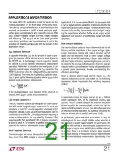
Error Amplifier and Internal Compensation
The buck-boost converter utilizes a voltage mode error
amplifierwithaninternalcompensationnetworkasshown
in Figure 3.
Notice that resistor R2 of the external resistor divider
networkplaysanintegralroleindeterminingthefrequency
response of the compensation network. The ratio of R2 to
R1 is set to program the desired output voltage but this
still allows the value of R2 to be adjusted to optimize the
When the input voltage is significantly greater than the
output voltage, the buck-boost converter operates in
buck mode. Switch D turns on continuously and switch
C remains off. Switches A (or A´) and B are pulse width
modulatedtoproducetherequireddutycycletosupportthe
output regulation voltage. As the input voltage decreases,
LTC3101
V
OUT3
L
V
OUT3
USB2 BAT2
A´
SW3A
SW3B
D
V
OUT3
R2
R1
+
–
0.599V
FB3
A
B
C
GND (EXPOSED PAD)
LTC3101
3101 F02
Figure 2. Buck-Boost Switch Topology
Figure 3. Buck-Boost Error Amplifier and Compensation
3101f
18

 Linear [ Linear ]