LTC3101
APPLICATIONS INFORMATION
The basic LTC3101 application circuit is shown as the
Typical Application on the front page of this data sheet.
The external component selection is dependent upon the
required performance of the IC in each particular appli-
cation given considerations and tradeoffs such as PCB
area, output voltages, output currents, ripple voltages
and efficiency. This section of the data sheet provides
some basic guidelines and considerations to aid in the
selection of external components and the design of the
application circuit.
application, it is recommended that it be bypassed with
a 1ꢀF or larger ceramic capacitor. There is no limit to the
maximumcapacitanceonthispin.However,thesoft-start
duration is formed by the current-limited output charg-
ing the capacitance attached to the pin so larger output
capacitors will result in proportionally longer soft-start
durations.
Buck Inductor Selection
The choice of buck inductor value influences both the ef-
ficiency and the magnitude of the output voltage ripple.
Larger inductance values will reduce inductor current
ripple and will therefore lead to lower output voltage
ripple. For a fixed DC resistance, a larger value inductor
will yield higher efficiency by lowering the peak current to
be closer to the average output current. However, a larger
inductor within a given inductor family will generally have
a greater series resistance, thereby counteracting this
efficiency advantage.
C
Capacitor Selection
RS
A capacitor from the C pin to ground is used to pro-
RS
gram the duration of the microprocessor reset signal on
the RESET pin. A low leakage ceramic capacitor should
be utilized to ensure reliable temperature independent
operation. At the start of the active-low reset pulse, a 1ꢀA
(typical) current begins charging the C capacitor. The
RS
RESET pulse ends when the voltage at the C pin reaches
RS
1.20V(typical).Therefore,therequiredC capacitorvalue,
RS
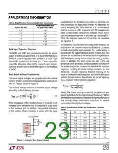
Given a desired peak-to-peak current ripple, ΔI , the
L
C , is given by the following equation where t
is the
RS
RESET
required inductance can be calculated via the following
expression, where f represents the switching frequency
in MHz:
desired reset duration in milliseconds:
tRESET
1200
CRS
=
μF
( )
⎛
⎞
VOUT
f • ΔIL
VOUT
L =
1–
μH
(
)
⎜
⎟
V
If the microprocessor reset function of the LTC3101 is
⎝
⎠
IN
unused, the C pin can be left unconnected.
RS
A reasonable choice for ripple current is ΔI = 140mA
L
LDO Output Capacitance
which represents 40% of the maximum 350mA load
current. The DC current rating of the inductor should be
at least equal to the maximum load current plus half the
ripple current in order to prevent core saturation and loss
of efficiency during operation. To optimize efficiency the
inductor should have a low DC resistance (DCR).
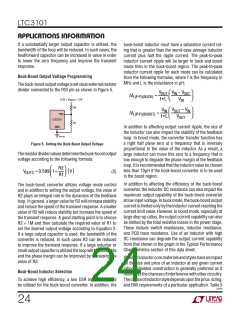
The LDO has been specifically designed for stable opera-
tion with a wide range of output capacitors. For most ap-
plications, a low ESR ceramic capacitor of at least 4.7μF
should be utilized. Large valued supercapacitors can be
connected directly to the LDO output without requiring a
series isolation resistor for loop stability. However, if the
supercapacitor has significant ESR, it may be necessary
to place a small 4.7ꢀF ceramic in parallel with the super-
capacitor to maintain an adequate phase margin.
In particularly space-restricted applications it may be
advantageous to use a much smaller value inductor at
the expense of larger ripple current. In such cases, the
converter will operate in discontinuous conduction for a
wider range of output loads and efficiency will be reduced.
In addition, there is a minimum inductor value required
to maintain stability of the current loop as determined by
the fixed internal slope compensation. Specifically, if the
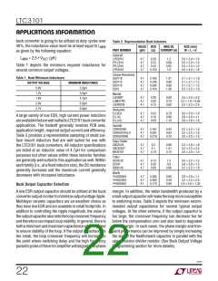
MAX Capacitor Selection
The MAX output serves as the input to the LDO. There-
fore, even if the MAX output is unused directly in the
3101f
21

 Linear [ Linear ]