LT8705
APPLICATIONS INFORMATION
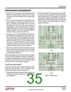
• Connecttheinputcapacitors,C ,andoutputcapacitors,
• Avoid running signal traces parallel to the traces that
carry high di/dt current because they can receive in-
ductivelycoupledvoltagenoise. ThisincludestheSW1,
SW2, TG1 and TG2 traces to the controller.
IN
C
, closely to the power MOSFETs. These capacitors
OUT
carry the MOSFET AC current in the boost and buck
regions.
• Connect the FBOUT and FBIN pin resistor dividers to
• Useimmediateviastoconnectthecomponents(includ-
ing the LT8705’s GND pins) to the ground plane. Use
several vias for each power component.
the (+) terminals of C
and C respectively. Small
OUT
IN
FBOUT/FBIN bypass capacitors may be connected
closely to the LT8705’s GND pin if needed. The resistor
connections should not be along the high current or
noise paths.
• Minimize parasitic SW pin capacitance by removing
GND and V copper from underneath the SW1 and
IN
SW2 regions.
• Route current sense traces (CSP/CSN, CSPIN/CSNIN,
CSPOUT/CSNOUT) together with minimum PC trace
spacing. Avoid having sense lines pass through noisy
areas,suchasswitchnodes.Theoptionalfilternetwork
capacitor between CSP and CSN should be as close as
possibletotheIC. Ensureaccuratecurrentsensingwith
• Except under the SW pin regions, flood all unused
areas on all layers with copper. Flooding with copper
will reduce the temperature rise of power components.
Connect the copper areas to a DC net (e.g., quiet GND).
• Partition the power ground from the signal ground. The
small-signal component grounds should not return to
the IC GND through the power ground path.
Kelvin connections at the R
resistors.
SENSE
• Connect the V pin compensation network closely to
C
• PlaceswitchM2andswitchM3asclosetothecontroller
the IC, between V and the signal ground pins. The
C
as possible, keeping the GND, BG and SW traces short.
capacitor helps to filter the effects of PCB noise and
output voltage ripple voltage from the compensation
loop.
• Minimize inductance from the sources of M2 and M3
to R
by making the trace short and wide.
SENSE
• Connect the INTV and GATEV bypass capacitors
CC
CC
• Keep the high dV/dT nodes SW1, SW2, BOOST1,
BOOST2,TG1andTG2awayfromsensitivesmall-signal
nodes.
close to the IC. The capacitors carry the MOSFET driv-
ers’ current peaks.
• Theoutputcapacitor(–)terminalsshouldbeconnected
as closely as possible to the (–) terminals of the input
capacitor.
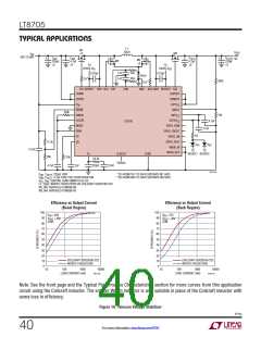
Design Example
V = 8V to 25V
IN
V
I
= 12V
OUT
• Connect the top driver boost capacitor, C , closely
B1
= 5A
to the BOOST1 and SW1 pins. Connect the top driver
OUT(MAX)
boost capacitor, C , closely to the BOOST2 and SW2
B2
f = 350kHz
pins.
Maximum ambient temperature = 60°C
8705p
36
For more information www.linear.com/8705

 Linear [ Linear ]