LT8705
APPLICATIONS INFORMATION
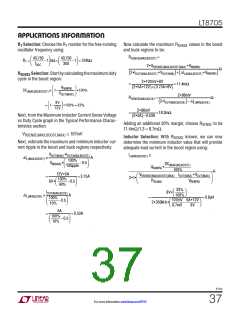
Loop Compensation
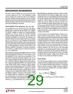
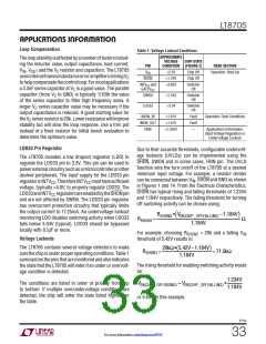
Table 1: Voltage Lockout Conditions
APPROXIMATE
Theloopstabilityisaffectedbyanumberoffactorsinclud-
ing the inductor value, output capacitance, load current,
VOLTAGE
CHIP STATE
PIN
CONDITION (FIGURE 2)
READ SECTION
V , V
and the V resistor and capacitors. The LT8705
IN OUT
C
V
<2.5V
<1.18V
<4.65V
Chip Off
Chip Off
Operation: Start-Up
IN
usesinternaltransconductanceerroramplifiersdrivingV
C
SHDN
INTV and
tohelpcompensatethecontrolloop.Formostapplications
Switcher
Off
CC
a 3.3nF series capacitor at V is a good value. The parallel
GATEV
CC
C
capacitor (from V to GND) is typically 1/10th the value
SWEN
LDO33
<1.18V
<3.04
Switcher
Off
C
of the series capacitor to filter high frequency noise. A
Switcher
Off
larger V series capacitor value may be necessary if the
C
output capacitance is reduced. A good starting value for
IMON_IN
IMON_OUT
FBIN
>1.61V
>1.61V
<1.205V
Fault
Fault
—
Operation: Fault Conditions
theV seriesresistoris20k.Lowerresistancewillimprove
C
stability but will slow the loop response. Use a trim pot
instead of a fixed resistor for initial bench evaluation to
determine the optimum value.
Applications Information:
Input Voltage Regulation or
Undervoltage Lockout
LDO33 Pin Regulator
Due to their accurate thresholds, configurable undervolt-
age lockouts (UVLOs) can be implemented using the
SHDN, SWEN and in some cases, FBIN pin. The UVLO
function sets the turn on/off of the LT8705 at a desired
minimum input voltage. For example, a resistor divider
The LT8705 includes a low dropout regulator (LDO) to
regulate the LDO33 pin to 3.3V. This pin can be used to
powerexternalcircuitrysuchasamicrocontrollerorother
desired peripherals. The input supply for the LDO33 pin
can be connected between V , SHDN and GND as shown
IN
regulatorisINTV .ThereforeINTV musthavesufficient
CC
CC
in Figures 1 and 14. From the Electrical Characteristics,
SHDN has typical rising and falling thresholds of 1.234V
and 1.184V respectively. The falling threshold for turning
off switching activity can be chosen using:
voltage, typically >4.0V, to properly regulate LDO33. The
LDO33andINTV regulatorsareenabledbytheSHDNpin
CC
and are not affected by SWEN. The LDO33 pin regulator
has overcurrent protection circuitry that typically limits
the output current to 17.25mA. An undervoltage lockout
monitoring LDO disables switching activity when LDO33
falls below 3.04V (typical). LDO33 should be bypassed
locally with 0.1µF or more.
RSHDN2 • V
–1.184V
(
)
(IN,CHIP _OFF,FALLING)
RSHDN1
=
Ω
1.184V
For example, choosing R
= 20k and a falling V
IN
SHDN2
Voltage Lockouts
threshold of 5.42V results in:
The LT8705 contains several voltage detectors to make
surethechipis underproperoperating conditions. Table 1
summarizesthepinsthataremonitoredandalsoindicates
the state that the LT8705 will enter if an under or overvolt-
age condition is detected.
20kΩ • 5.42V –1.184V
(
)
= 71.5kΩ
RSHDN1
=
1.184V
The rising threshold for enabling switching activity would
be:
1.234V
1.184V
The conditions are listed in order of priority from top
to bottom. If multiple over/undervoltage conditions are
detected, the chip will enter the state listed highest on
the table.
V
(IN,CHIP _OFF,RISING) = V
•
(IN,CHIP _OFF,FALLING)
or 5.65V in this example.
8705p
33
For more information www.linear.com/8705

 Linear [ Linear ]