LT8705
APPLICATIONS INFORMATION
Junction Temperature Measurement
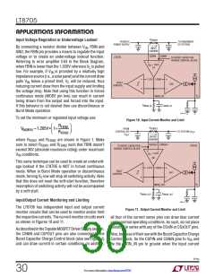
Similarcalculationscanbeusedtoselectaresistordivider
connectedtoSWENthatwouldstopswitchingactivitydur-
ing an undervoltage condition. Make sure that the divider
doesn’t cause SWEN to exceed 7V (absolute maximum
ThedutycycleoftheCLKOUTsignalislinearlyproportional
tothediejunctiontemperature, T . Measurethedutycycle
J
of the CLKOUT signal and use the following equation to
rating) under maximum V conditions. Using the FBIN
IN
approximate the junction temperature:
pin as an undervoltage lockout is discussed in the Input
DCCLKOUT –34.4%
Voltage Regulation or Undervoltage Lockout section.
TJ ≅
°C
0.325%
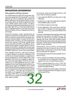
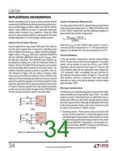
Inductor Current Sense Filtering
where DC
is the CLKOUT duty cycle in % and T
CLKOUT
J
Certain applications may require filtering of the inductor
current sense signals due to excessive switching noise
is the die junction temperature in °C. The actual die tem-
perature can deviate from the above equation by 10°C
thatcanappearacrossR
. Higheroperatingvoltages,
SENSE
higher values of R
, and more capacitive MOSFETs
SENSE
Thermal Shutdown
will all contribute additional noise across R
when
SENSE
If the die junction temperature reaches approximately
165°C, the part will go into thermal shutdown. The power
switch will be turned off and the INTV and LDO33
regulators will be turned off (see Figure 2). The part will
be re-enabled when the die temperature has dropped by
~5°C (nominal). After re-enabling, the part will start in
the switcher off state as shown in Figure 2. The part will
then initialize, perform a soft-start, then enter normal
operation as long as the die temperature remains below
approximately 165°C.
the SW pins transition. The CSP/CSN sense signals can
be filtered by adding one of the RC networks shown in
Figures 12a and 12b. Most PC board layouts can be drawn
to accommodate either network on the same board. The
network should be placed as close as possible to the IC.
The network in Figure 12b can reduce common mode
noise seen by the CSP and CSN pins of the LT8705 at the
expense of some increased ground trace noise as current
passesthroughthecapacitors.Ashortdirectpathfromthe
capacitor grounds to the IC ground should be used on the
PC board. Resistors greater than 10Ω should be avoided
as this can increase offset voltages at the CSP/CSN pins.
The RC product should be kept to less than 30ns.
CC
Efficiency Considerations
Theefficiencyofaswitchingregulatorisequaltotheoutput
power divided by the input power times 100%. It is often
useful to analyze individual losses to determine what is
limiting the efficiency and which change would produce
the most improvement. Although all dissipative elements
in the circuit produce losses, four main sources account
for most of the losses in LT8705 circuits:
10Ω
CSP
LT8705
R
SENSE
1nF
10Ω
CSN
8705 F12a
(12a)
1. Switching losses. These losses arises from the brief
amount of time switch M1 or switch M3 spends in the
saturatedregionduringswitchnodetransitions. Power
lossdependsupontheinputvoltage,loadcurrent,driver
strength and MOSFET capacitance, among other fac-
tors. See the Power MOSFET Selection and Efficiency
Considerations section for more details.
10Ω
CSP
CSN
LT8705
R
SENSE
1nF
10Ω
1nF
8705 F12b
(12b)
Figure 12. Inductor Current Sense Filter
8705p
34
For more information www.linear.com/8705

 Linear [ Linear ]