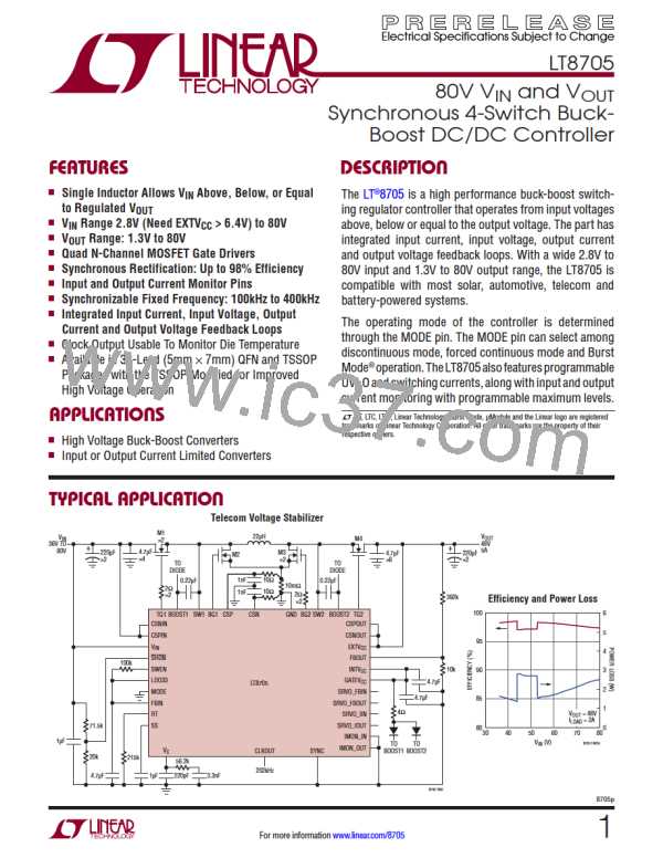
LT8705
APPLICATIONS INFORMATION
2. DC I R losses. These arise from the resistances of the
2
• The high di/dt path formed by switch M1, switch M2,
MOSFETs, sensing resistors, inductor and PC board
traces and cause the efficiency to drop at high output
currents.
D1, R
and the C capacitor should be compact
SENSE IN
with short leads and PC trace lengths. The high di/dt
path formed by switch M3, switch M4, D2 and the C
OUT
capacitor also should be compact with short leads and
PC trace lengths. Two layout examples are shown in
Figures 13a and 13b.
3. INTV current. This is the sum of the MOSFET driver
CC
current, LDO33 pin current and control currents. The
INTV regulator’s input voltage times the current
CC
represents lost power. This loss can be reduced by
V
IN
SW1
SW2
V
OUT
supplyingINTV currentthroughtheEXTV pinfrom
CC
CC
L
a high efficiency source, such as the output or alternate
supply if available. Also, lower capacitance MOSFETs
can reduce INTV current and power loss.
CC
4. C and C
loss. The input capacitor has the difficult
OUT
IN
D1
D2
C
job of filtering the large RMS input current to the regu-
lator in buck mode. The output capacitor has the more
difficult job of filtering the large RMS output current in
M1
M2
M3
M4
C
boost mode. Both C and C
are required to have
IN
OUT
IN
OUT
2
low ESR to minimize the AC I R loss and sufficient
capacitance to prevent the RMS current from causing
additional upstream losses in fuses or batteries.
R
SENSE
LT8705
CKT
GND
8705 F13a
5. Other losses. Schottky diodes D1 and D2 are respon-
sible for conduction losses during dead time and light
load conduction periods. Inductor core loss occurs
predominately at light loads.
(13a)
V
SW1
SW2
V
OUT
IN
L
D2
Whenmakingadjustmentstoimproveefficiency,theinput
current is the best indicator of changes in efficiency. If
one makes a change and the input current decreases, then
the efficiency has increased. If there is no change in input
current, then there is no change in efficiency.
M1
M4
D1
M2
M3
C
C
OUT
IN
Circuit Board Layout Checklist
The basic circuit board layout requires a dedicated ground
plane layer. Also, for high current, a multilayer board
provides heat sinking for power components.
R
SENSE
LT8705
CKT
GND
8705 F13b
• The ground plane layer should not have any traces and
should be as close as possible to the layer with the
power MOSFETs.
(13b)
Figure 13. Switches Layout
8705p
35
For more information www.linear.com/8705

 Linear [ Linear ]