LT8705
APPLICATIONS INFORMATION
Input Voltage Regulation or Undervoltage Lockout
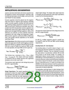
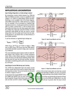
R
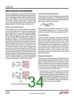
SENSE1
FROM DC
POWER SUPPLY
TO REMAINDER
OF SYSTEM
By connecting a resistor divider between V , FBIN and
IN
INPUT
CURRENT
GND, the FBIN pin provides a means to regulate the input
voltage or to create an undervoltage lockout function.
Referring to error amplifier EA3 in the Block Diagram,
CSPIN
CSNIN
LT8705
TO BOOST CAPACITOR
CHARGE CONTROL BLOCK
+
–
Ω
g
= 1m
A7
m
when FBIN is lower than the 1.205V reference V is pulled
C
low. For example, if V is provided by a relatively high
IN
impedancesource(i.e.,asolarpanel)andthecurrentdraw
–
+
1.61V 1.208V
+
–
pulls V below a preset limit, V will be reduced, thus
IN
C
FAULT
CONTROL
EA2
reducing current draw from the input supply and limiting
the voltage drop. Note that using this function in forced
continuous mode (MODE pin low) can result in current
being drawn from the output and forced into the input.
If this behavior is not desired then use discontinuous or
Burst Mode operation.
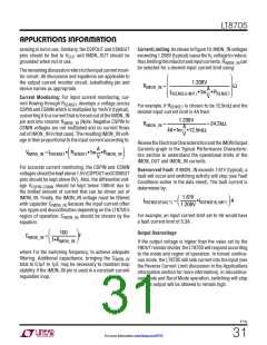
V
C
IMON_IN
R
C
IMON_IN
IMON_IN
8705 F10
To set the minimum or regulated input voltage use:
Figure 10. Input Current Monitor and Limit
RFBIN1
R
R
SENSE2
FROM
V
IN(MIN) = 1.205V • 1+
CONTROLLER
TO SYSTEM V
OUT
FBIN2
V
OUT
OUTPUT
CURRENT
where R
sure to select R
and R
are shown in Figure 1. Make
FBIN1
FBIN2
and R
CSPOUT CSNOUT
such that FBIN doesn’t
LT8705
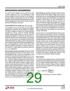
TO BOOST CAPACITOR
CHARGE CONTROL BLOCK
FBIN1
FBIN2
exceed 30V (absolute maximum rating) under maximum
+
–
Ω
g
= 1m
A8
m
V conditions.
IN
This same technique can be used to create an undervolt-
age lockout if the LT8705 is NOT in forced continuous
mode. When in Burst Mode operation or discontinuous
–
+
1.61V 1.208V
+
–
FAULT
CONTROL
EA1
mode, forcing V low will stop all switching activity. Note
C
that this does not reset the soft-start function, therefore
resumption of switching activity will not be accompanied
by a soft-start.
V
IMON_OUT
C
R
C
IMON_OUT
IMON_OUT
Input/Output Current Monitoring and Limiting
8705 F11
The LT8705 has independent input and output current
monitor circuits that can be used to monitor and/or limit
the respective currents. The current monitor circuits work
as shown in Figures 10 and 11.
Figure 11. Output Current Monitor and Limit
all four of the current sense pins can draw bias current
under normal operating conditions. As such, do not place
resistors in series with any of the CSxIN or CSxOUT pins.
AsdescribedintheTopsideMOSFETDriverSupplysection,
the CSNIN and CSPOUT pins are also connected to the
Boost Capacitor Charge Control block (also see Figure 1)
and can draw current in certain conditions. In addition,
Also, becauseoftheirusewiththeBoostCapacitorCharge
Control block, tie the CSPIN and CSNIN pins to V and
IN
tie the IMON_IN pin to ground when the input current
8705p
30
For more information www.linear.com/8705

 Linear [ Linear ]