LT8705
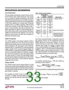
APPLICATIONS INFORMATION
can have a reverse voltage up to V and D2 can have
Boost Diodes D and D : Although Schottky diodes
B1 B2
IN
a reverse voltage up to V . The combination of high
have the benefit of low forward voltage drops, they can
exhibithighreversecurrentleakageandhavethepotential
for thermal runaway under high voltage and temperature
conditions. Silicon diodes are thus recommended for
OUT
reverse voltage and current can lead to self heating of
the diode. Besides reducing efficiency, this can increase
leakagecurrentwhichincreasestemperaturesevenfurther.
Choose packages with lower thermal resistance (θ ) to
minimize self heating of the diodes.
diodes D and D . Make sure that D and D have
JA
B1 B2 B1 B2
reverse breakdown voltage ratings higher than V
IN(MAX)
and V
and have less than 1mA of reverse leakage
OUT(MAX)
Topside MOSFET Driver Supply (C , D , C , D )
current at the maximum operating junction temperature.
Make sure that the reverse leakage current at high op-
erating temperatures and voltages won’t cause thermal
runaway of the diode.
B1 B1 B2 B2
ThetopMOSFETdrivers(TG1andTG2)aredrivendigitally
between their respective SW and BOOST pin voltages.
The BOOST voltages are biased from floating bootstrap
capacitors C and C , which are normally recharged
In some cases it is recommended that up to 5Ω of resis-
tance is placed in series with D and D . The resistors
B1
B2
through external silicon diodes D and D when the
B1
B2
B1
B2
respective top MOSFET is turned off. The capacitors are
reducesurgecurrentsinthediodesandcanreduceringing
at the SW and BOOST pins of the IC. Since SW pin ringing
is highly dependent on PCB layout, SW pin edge rates and
the type of diodes used, careful measurements directly
at the SW pins of the IC are recommended. If required, a
chargedtoabout6.3V(aboutequaltoGATEV )forcingthe
CC
V
and V
voltages to be about 6.3V.
The boost capacitors C and C need to store about 100
BOOST1-SW1
BOOST2-SW2
B1
B2
timesthegatechargerequiredbythetopswitchesM1and
M4. In most applications, a 0.1μF to 0.47μF, X5R or X7R
dielectric capacitor is adequate. The bypass capacitance
single resistor can be placed between GATEV and the
CC
common anodes of D and D (as in the front page
B1
B2
from GATEV to GND should be at least ten times the
application) or by placing separate resistors between the
CC
C
B1
or C capacitance.
cathodes of each diode and the respective BOOST pins.
B2
ExcessiveresistanceinserieswithD andD canreduce
B1
B2
BoostCapacitorChargeControlBlock:WhentheLT8705
operates exclusively in the buck or boost region, one of
the top MOSFETS, M1 or M4, can be constantly on. This
the BOOST-SW capacitor voltage when the M2 or M3
on-times are very short and should be avoided.
prevents the respective bootstrap capacitor, C or C ,
B1
B2
Output Voltage
from being recharged through the silicon diode, D or
B1
D . The Boost Capacitor Charge Control block (see Fig-
The LT8705 output voltage is set by an external feedback
resistivedividercarefullyplacedacrosstheoutputcapaci-
tor. The resultant feedback signal (FBOUT) is compared
with the internal precision voltage reference (typically
1.207V) by the error amplifier EA4. The output voltage is
given by the equation:
B2
ure 1) keeps the appropriate BOOST pin charged in these
cases. When the M1 switch is always on (boost region),
current is automatically drawn from the CSPOUT and/or
BOOST2 pins to charge the BOOST1 capacitor as needed.
When the M4 switch is always on (buck region) current
is drawn from the CSNIN and/or BOOST1 pins to charge
the BOOST2 capacitor. Because of this function, CSPIN
and CSNIN should be connected to a potential close to
RFBOUT1
R
VOUT = 1.207V • 1+
FBOUT2
V . Tie both pins to V if they are not being used. Also,
IN
IN
where R
and R
are shown in Figure 1.
FBOUT1
FBOUT2
CSPOUT and CSNOUT should always be tied to a potential
close to V , or be tied directly to V if not being used.
OUT
OUT
8705p
29
For more information www.linear.com/8705

 Linear [ Linear ]