LT3580
APPLICATIONS INFORMATION
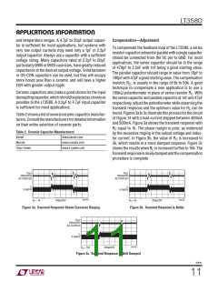
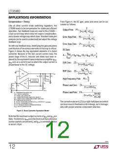
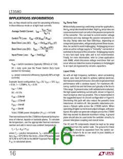
Compensation—Theory
From Figure 4, the DC gain, poles and zeros can be cal-
culated as follows:
Like all other current mode switching regulators, the
LT3580 needs to be compensated for stable and efficient
operation. Two feedback loops are used in the LT3580—
a fast current loop which does not require compensation,
and a slower voltage loop which does. Standard bode plot
analysis can be used to understand and adjust the voltage
feedback loop.
2
Output Pole: P1=
2• ꢀ •RL •COUT
1
Error AmpPole: P2=
2• ꢀ •RO •CC
1
Error Amp Zero: Z1=
As with any feedback loop, identifying the gain and phase
contribution of the various elements in the loop is critical.
Figure 4 shows the key equivalent elements of a boost
converter. Because of the fast current control loop, the
power stage of the IC, inductor and diode have been re-
2• ꢀ •RC •CC
DC Gain:
VREF
1
4
A =
• V •gma •RO •gmp •RL •
IN
2
VOUT
placed by the equivalent transconductance amplifier g
.
mp
1
g
acts as a current source where the output current is
mp
ESR Zero: Z2=
RHP Zero: Z3=
2• ꢀ •RESR •COUT
proportional to the VC voltage.
–
V
2 •RL
2• ꢀ • VOUT2 •L
IN
g
mp
V
OUT
+
C
R
R
L
PL
ESR
fS
3
HighFrequency Pole: P3>
C
OUT
1.215V
REFERENCE
+
–
V
C
g
ma
R1
R2
1
R
R
O
Phase Lead Zero: Z4=
C
2• ꢀ •R1•CPL
C
C
3580 F04
1
C : COMPENSATION CAPACITOR
Phase Lead Pole: P4=
C
C
C
g
: OUTPUT CAPACITOR
R1•R2
R1+R2
OUT
2• ꢀ •CPL •
: PHASE LEAD CAPACITOR
PL
ma
mp
: TRANSCONDUCTANCE AMPLIFIER INSIDE IC
: POWER STAGE TRANSCONDUCTANCE AMPLIFIER
g
R : COMPENSATION RESISTOR
C
R : OUTPUT RESISTANCE DEFINED AS V
DIVIDED BY I
LOAD(MAX)
Thecurrentmodezero(Z3)isaright-halfplanezerowhich
canbeanissueinfeedbackcontroldesign, butismanage-
able with proper external component selection.
L
O
OUT
R : OUTPUT RESISTANCE OF g
ma
R1, R2: FEEDBACK RESISTOR DIVIDER NETWORK
: OUTPUT CAPACITOR ESR
R
ESR
Figure 4. Boost Converter Equivalent Model
Note that the ma ximum output currents of g andg are
mp
ma
finite.Thelimitsforg areintheElectricalCharacteristics
mp
section (switch current limit), and g is nominally limited
ma
to about 12μA.
3580fc
12

 Linear [ Linear ]