LT3580
APPLICATIONS INFORMATION
tion, so they should not be used for calculating efficiency
in discontinuous mode or at light load currents.
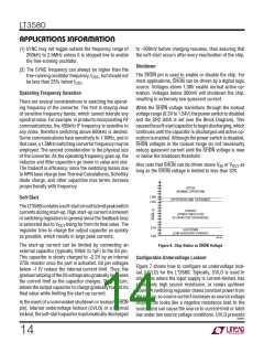
V Ramp Rate
IN
While initially powering a switching converter application,
theV ramprateshouldbelimited.HighV rampratescan
VOUT •IOUT
IN
IN
Average Switch Current: ISW
=
causeexcessiveinrushcurrentsinthepassivecomponents
of the converter. This can lead to current and/or voltage
overstress and may damage the passive components or
the chip. Ramp rates less than 500mV/μs, depending on
componentparameters,willgenerallypreventtheseissues.
Also, be careful to avoid hotplugging. Hotplugging occurs
when an active voltage supply is “instantly” connected or
switchedtotheinputoftheconverter. Hotpluggingresults
in very fast input ramp rates and is not recommended.
Finally, for more information, refer to Linear application
note AN88, which discusses voltage overstress that can
occur when an inductive source impedance is hotplugged
to an input pin bypassed by ceramic capacitors.
V • ꢀ
IN
Switch I2R Loss: PSW =(DC)(ISW)2(RSW
Base Drive Loss (AC): PBAC =13n(ISW)(VOUT )(f)
)
(V )(ISW)(DC)
IN
Base Drive Loss (DC): PBDC
=
50
Input Power Loss: PINP = 7mA(V )
IN
where:
R
SW
= switch resistance (typically 200mΩ at 1.5A)
DC = duty cycle (see the Power Switch Duty Cycle
section for formulas)
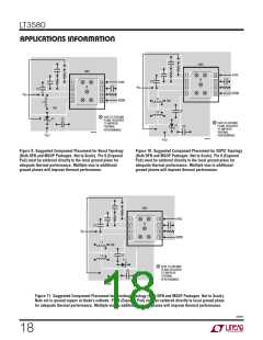
Layout Hints
η = power conversion efficiency (typically 88% at high
As with all high frequency switchers, when considering
layout, care must be taken to achieve optimal electrical,
thermalandnoiseperformance.Onewillnotgetadvertised
performance with a careless layout. For maximum effi-
ciency, switch rise and fall times are typically in the 5ns to
10nsrange.Topreventnoise,bothradiatedandconducted,
the high speed switching current path, shown in Figure 8,
must be kept as short as possible. This is implemented in
the suggested layout of a boost configuration in Figure 9.
Shortening this path will also reduce the parasitic trace
inductance. At switch-off, this parasitic inductance pro-
duces a flyback spike across the LT3580 switch. When
operatingathighercurrentsandoutputvoltages,withpoor
layout, thisspikecangeneratevoltagesacrosstheLT3580
that may exceed its absolute maximum rating. A ground
plane should also be used under the switcher circuitry to
prevent interplane coupling and overall noise.
currents)
Example: boost configuration, V = 5V, V
= 12V, I
OUT
IN
OUT
= 0.5A, f = 1.25MHz, V = 0.5V:
D
I
= 1.36A
SW
DC = 61.5%
P
P
P
P
= 228mW
= 270mW
= 84mW
= 35mW
SW
BAC
BDC
INP
Total LT3580 power dissipation (P ) = 617mW
TOT
ThermalresistancefortheLT3580isinfluencedbythepres-
ence of internal, topside or backside planes. To calculate
die temperature, use the appropriate thermal resistance
number and add in worst-case ambient temperature:
The VC and FB components should be kept as far away
as practical from the switch node. The ground for these
components should be separated from the switch cur-
rent path. Failure to do so can result in poor stability or
subharmonic oscillation.
T = T + θ • P
TOT
J
A
JA
where T = junction temperature, T = ambient tempera-
J
A
ture, θ = 43°C/W for the 3mm × 3mm DFN package and
JA
35°C/W to 40°C/W for the MSOP Exposed Pad package.
P
is calculated above.
TOT
3580fc
16

 Linear [ Linear ]