LT3580
APPLICATIONS INFORMATION
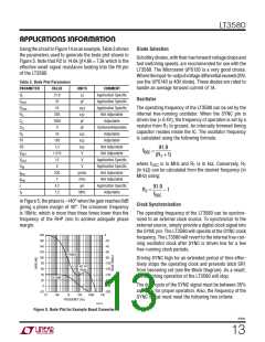
Setting Output Voltage
Inductor Selection
The output voltage is set by connecting a resistor (R )
General Guidelines: The high frequency operation of the
LT3580allowsfortheuseofsmallsurfacemountinductors.
For high efficiency, choose inductors with high frequency
core material, such as ferrite, to reduce core losses. To
improve efficiency, choose inductors with more volume
for a given inductance. The inductor should have low DCR
FB
from V
to the FB pin. R is determined from the
OUT
FB
following equation:
|VOUT ꢀ VFB |
RFB =
83.3μA
2
(copperwireresistance)toreduceI Rlosses,andmustbe
where V is 1.215V (typical) for non-inverting topologies
FB
able to handle the peak inductor current without saturat-
ing. Note that in some applications, the current handling
requirements of the inductor can be lower, such as in the
SEPIC topology, where each inductor only carries a frac-
tion of the total switch current. Molded chokes or chip
inductors usually do not have enough core area to sup-
port peak inductor currents in the 2A to 3A range. To
minimize radiated noise, use a toroidal or shielded induc-
tor. Note that the inductance of shielded types will drop
more as current increases, and will saturate more easily.
See Table 1 for a list of inductor manufacturers.
(i.e., boost and SEPIC regulators) and 5mV (typical) for
inverting topologies (see the Electrical Characteristics).
Power Switch Duty Cycle
In order to maintain loop stability and deliver adequate
current to the load, the power NPN (Q1 in the Block Dia-
gram) cannot remain “on” for 100% of each clock cycle.
The maximum allowable duty cycle is given by:
(TP ꢀMinOffTime)
DCMAX
=
•100%
TP
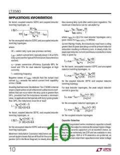
Table 1.Inductor Manufacturers
where T is the clock period and Min Off Time (found in
P
Coilcraft
DO3316P, MSS7341 and LPS4018
Series
www.coilcraft.com
the Electrical Characteristics) is typically 60ns.
Coiltronics DR, LD and CD Series
www.coiltronics.com
www.murata.com
www.sumida.com
The application should be designed so that the operating
Murata
Sumida
LQH55D and LQH66S Series
duty cycle does not exceed DC
.
MAX
CDRH5D18B/HP, CDR6D23MN,
CDRH6D26/HP, CDRH6D28,
CDR7D28MN and CDRH105R Series
Duty cycle equations for several common topologies are
given below, where V is the diode forward voltage drop
D
and V
is typically 300mV at 1.5A.
TDK
RLF7030 and VLCF4020 Series
WE-PD and WE-PD2 Series
www.tdk.com
CESAT
Würth
www.we-online.com
For the boost topology:
OUT ꢁ V + VD
Minimum Inductance: Although there can be a tradeoff
with efficiency, it is often desirable to minimize board
space by choosing smaller inductors. When choosing an
inductor, there are two conditions that limit the minimum
inductance; (1) providing adequate load current, and (2)
avoidance of subharmonic oscillation.
V
IN
DC ꢀ
V
OUT + VD ꢁ VCESAT
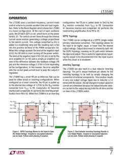
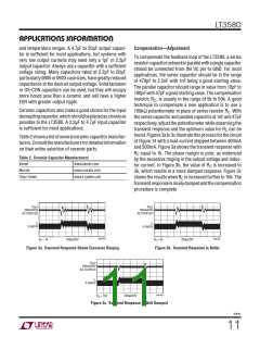
For the SEPIC or dual inductor inverting topology (see
Figures 1 and 2):
VD+|VOUT
V + |VOUT | + VD ꢁ VCESAT
|
DC ꢀ
Adequate Load Current: Small value inductors result in
increased ripple currents and thus, due to the limited peak
switch current, decrease the average current that can be
IN
The LT3580 can be used in configurations where the duty
cycle is higher than DC , but it must be operated in
provided to a load (I ). In order to provide adequate
MAX
OUT
the discontinuous conduction mode so that the effective
duty cycle is reduced.
load current, L should be at least:
DC • V
IN
L >
ꢂ
ꢄ
ꢃ
OUT ꢅ
|VOUT |• I
2(f) ILIM ꢀ
ꢇ
V • ꢁ
ꢆ
IN
3580fc
9

 Linear [ Linear ]