LT3580
APPLICATIONS INFORMATION
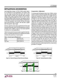
for boost, coupled inductor SEPIC and coupled inductor
inverting topologies, or:
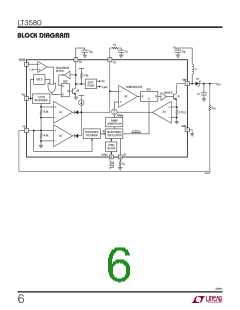
thus causing duty cycle jitter and/or poor regulation. The
maximum inductance can be calculated by:
DC • V
VIN – VCESAT
IMINꢀRIPPLE
DC
f
IN
L1 L2>
LMAX
=
•
ꢂ
ꢅ
ꢀ IOUT ꢇ
ꢆ
VOUT • IOUT
2(f) ꢄILIM ꢀ
V • ꢁ
ꢃ
IN
where L
is L1||L2 for dual inductor topologies and a
MAX
good choice for I
is 300mA.
MIN-RIPPLE
for the uncoupled inductor SEPIC and uncoupled inductor
inverting topologies.
Current Rating: Finally, the inductor(s) must have a rating
greater than its peak operating current to prevent inductor
saturation resulting in efficiency loss. In steady state, the
peakinputinductorcurrent(continuousconductionmode
only) is given by:
where:
DC = switch duty cycle (see previous section)
I
= switch current limit, typically about 2.4A at 50%
dutycycle(seetheTypicalPerformanceCharacteristics
LIM
VOUT •IOUT
V •DC
2•L1• f
IN
section).
IL1ꢀPEAK
=
+
V • ꢁ
IN
η = power conversion efficiency (typically 88% for
boost and 75% for dual inductor topologies at high
currents).
for the boost, uncoupled inductor SEPIC and uncoupled
inductor inverting topologies, or:
|VOUT •IOUT
|
V •DC
f = switching frequency
IN
IL1ꢀPEAK ꢁ
+
V • ꢂ•DC 2•L1• f
IN
Negative values of L
indicate that the output load
MIN1
current I
exceeds the switch current limit capability
OUT
for the coupled inductor SEPIC and coupled inductor
inverting topology.
of the LT3580.
AvoidingSubharmonicOscillations:TheLT3580’sinternal
slopecompensationcircuitwillpreventsubharmonicoscil-
lations that can occur when the duty cycle is greater than
50%, provided that the inductance exceeds a minimum
value. In applications that operate with duty cycles greater
than 50%, the inductance must be at least:
For dual inductor topologies, the peak output inductor
current is given by:
VOUT • 1–DC
(
)
IL2ꢀPEAK =IOUT +
2•L2• f
for the uncoupled inductor topologies, or
V • 2•DC –1
(1ꢀDC)•(f)•0.8
(
)
IN
L >
VOUT • 1–DC
(
)
IOUT
1–DC
I
L2ꢀPEAK ꢁ
+
2•L2• f
for boost, coupled inductor SEPIC, and coupled inductor
inverting topologies, or:
for the coupled inductor topologies
V • 2•DC –1
(1ꢀDC)•(f)•0.8
(
)
IN
L1 L2>
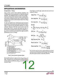
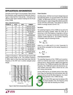
Capacitor Selection
Low ESR (equivalent series resistance) capacitors should
beusedattheoutputtominimizetheoutputripplevoltage.
Multilayer ceramic capacitors are an excellent choice, as
they have an extremely low ESR and are available in very
small packages. X5R or X7R dielectrics are preferred, as
thesematerialsretaintheircapacitanceoverwidervoltage
for the uncoupled inductor SEPIC and uncoupled inductor
inverting topologies.
Maximum Inductance: Excessive inductance can reduce
currentrippletolevelsthataredifficultforthecurrentcom-
parator (A3 in the Block Diagram) to cleanly discriminate,
3580fc
10

 Linear [ Linear ]