LT3587
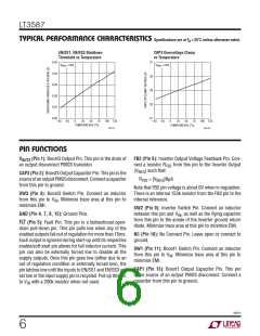
PIN FUNCTIONS
V
(Pin 14): Boost1 Output Pin. This pin is the drain
V
(Pin 20): Boost3 Output Voltage Feedback Pin. Con-
OUT1
FB3
of an output disconnect PMOS transistor.
nect a resistor R
such that:
from this pin to V
(or CAP3)
VFB3
OUT3
FB1 (Pin 15): Boost1 Output Voltage Feedback Pin. Con-
nect a resistor R
such that:
from this pin to V
(or CAP1)
R
= ((V /0.8V) – 1) • 56.3k
VOUT3
FB1
OUT1
VFB3
There is an internal 56.3k resistor from the V
pin to
VFB3
FB3
R
= ((V /1.22V) – 1) • 88.5k
VOUT1
ground. In the current regulator configuration, R
can
FB1
be optionally used to limit the maximum output voltage
There is an internal 88.5k resistor from the FB1 pin to
ground.
to V
, such that:
CLAMP
R
= ((V
/0.8V) – 1) • 56.3k
CLAMP
VFB3
EN/SS1(Pin16):Boost1/InverterShutdownandSoft-Start
Pin. Boost1 and Inverter are enabled when the voltage
on this pin is greater than 2.5V. They are disabled when
the voltage is below 0.2V. An internal 1μA current source
in conjunction with an external capacitor can be used to
ramp this pin and provide soft-start.
Note: When no voltage clamp is desired in the current
regulator configuration, tie V to GND.
FB3
ExposedPad(Pin21):GroundPin.ConnecttoPCBground
plane.Groundplaneconnectionthroughmultipleviasunder
the package is recommended for optimum electrical and
thermal performance.
V (Pin 17): Input Supply Pin. Must be locally bypassed
IN
with an X5R or X7R type ceramic capacitor.
EN/SS3 (Pin 18): Boost3 Shutdown and Soft-Start Pin.
Boost3 is enabled when the voltage on this pin is greater
than 2V. It is disabled when the voltage is below 0.2V. An
internal 1μA current source in conjunction with an exter-
nal capacitor can be used to ramp this pin and provide
soft-start.
I
(Pin 19): Boost3 Output Current Programming Pin.
FB3
Connect a resistor R
from this pin to ground such
IFB3
that:
R
= 200 • (0.8V/I
)
IFB3
VOUT3
If Boost3 output is configured as a voltage regulator,
can be optionally used to limit the maximum output
R
IFB3
current to I
:
LIMIT
R
IFB3
= 200 • (0.8V/I
)
LIMIT
Note: Tie I to GND when no current limit is desired.
FB3
3587fc
7

 Linear [ Linear ]