LT3694/LT3694-1
APPLICATIONS INFORMATION
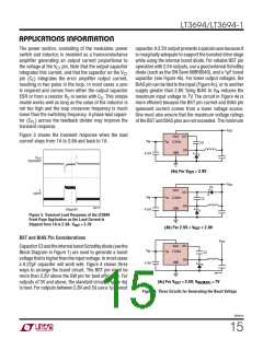
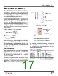
5.0
4.8
4.6
4.4
4.2
4.0
3.8
3.6
3.4
3.2
3.0
operating voltage of an LT3694 application is limited by
the minimum input voltage (4V) and by the maximum
duty cycle as outlined in a previous section. For proper
start-up, the minimum input voltage is also limited by the
boost circuit. If the input voltage is ramped slowly, or the
LT3694 is turned on with its EN/UVLO or TRK/SS pin when
theoutputisalreadyinregulation,thentheboostcapacitor
may not be fully charged. Because the boost capacitor is
charged with the energy stored in the inductor, the circuit
will rely on some minimum load current to get the boost
circuit running properly. This minimum load will depend
on input and output voltages, and on the arrangement of
the boost circuit. The minimum load generally goes to
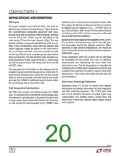
zero once the circuit has started. Figure 5 shows a plot
of input voltage to start and to run as a function of load
current. In many cases the discharged output capacitor
will present a load to the switcher, which will allow it to
start. The plots show the worst-case situation in which
V
f
= 3.3V
OUT
SW
TO START
TO RUN
= 800kHz
0.001
0.01
0.1
1
LOAD CURRENT (A)
7.0
6.5
6.0
5.5
5.0
4.5
4.0
V
SW
= 5V
OUT
f
= 800kHz
TO START
TO RUN
V is ramping very slowly. For lower start-up voltage, the
IN
boost diode can be tied to V , however, this restricts the
IN
input range to one-half of the absolute maximum rating
of the BST pin.
0.001
0.01
0.1
1
At light loads, the inductor current becomes discontinu-
ous and the effective duty cycle can be very high. This
reduces the minimum input voltage to approximately
LOAD CURRENT (A)
36941 F05
Figure 5. The Minimum Input Voltage Depends on
Output Voltage, Load Current and Boost Circuit
300mV above V . At higher load currents, the inductor
OUT
current is continuous and the duty cycle is limited by the
maximum duty cycle of the LT3694, requiring a higher
input voltage to maintain regulation.
Enable and Programmable Undervoltage Lockout
The EN/UVLO pin provides both logic enable and pro-
grammable undervoltage lockout functions. There are
two thresholds on the EN/UVLO pin. The first threshold is
at 500mV (typ). When EN/UVLO is below this threshold,
the LT3694 is in complete shutdown and the quiescent
current drops below 2µA.
Internal Undervoltage Lockout
The LT3694 features an internal undervoltage lockout that
will shut off all three regulators if the input voltage drops
toolowtomaintainregulationoftheinternalcircuitry. This
lockout trips when V drops below 3.8V (typ).
IN
36941fb
16

 Linear [ Linear ]