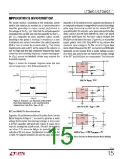
LT3694/LT3694-1
APPLICATIONS INFORMATION
If the current feeding the collector of the NPN through the
sense resistor comes from a supply that is not connected
to BIAS, the current limit cannot be used and the LIM pin
must be connected to BIAS to disable the current limit.
Shorted and Reversed Input Protection
If an inductor is chosen that will not saturate excessively,
an LT3694 buck regulator will tolerate a shorted output.
There is another situation to consider in systems where
the output will be held high when the input to the LT3694
is absent. This may occur in battery charging applications
or in battery backup systems where a battery or some
other supply is diode ORed with the LT3694’s output. If
Tracking and Soft-Start
The output of the LT3694 regulates to the lowest voltage
present at either the TRK/SS pin or an internal 0.75V
reference. A capacitor from the TRK/SS pin to ground is
charged by an internal 3μA current source resulting in a
linear output ramp from 0V to the regulated output whose
duration is given by:
the V pin is allowed to float and the EN/UVLO pin is held
IN
high (either by a logic signal or because it is tied to V ),
IN
then the LT3694’s internal circuitry will pull its quiescent
current through its SW pin. This is fine if the system
can tolerate a few mA in this state. If the EN/UVLO pin
is grounded, the SW pin current will drop to essentially
CTRKSS •0.75V
tRAMP
=
3µA
zero. However, if the V pin is grounded while the output
IN
is held high, then parasitic diodes inside the LT3694 can
At power-up or at any shutdown event, the TRK/SS pins
are internally pulled to ground through 100Ω to insure
the soft-start capacitors are discharged. The pins clamp
at 1.3V.
pull large currents from the output through the SW pin
and the V pin. The circuit in Figure 8 runs only when the
IN
input voltage is present—and protects against a shorted
or reversed input.
Ratiometric tracking is achieved by tying the TRK/SS pins
tied together and connecting to a single capacitor. The
charge current is multiplied by the number of TRK/SS
pins connected.
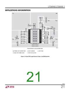
D4
V
V
BST
SW
IN
IN
LT3694
EN/UVLO
V
OUT
V
C
Coincident tracking is accomplished by adding an addi-
tional resistor divider to the master regulator output and
connecting it to the TRK/SS pin of the slave regulator. The
resistor divider should be equal to the slave’s feedback
GND FB
BACKUP
divider. Keep in mind that the LDO pass transistor V
CE(SAT)
36941 F08
will limit how well the LDO output can coincidentally track
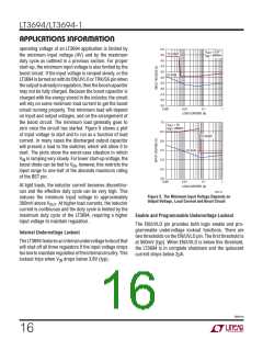
Figure 8. Diode D4 Prevents a Shorted Input from
the switching regulator output.
Discharging a Backup Battery Tied to the Output. It Also
Protects the Circuit from a Reversed Input. The LT3694
Runs Only When the Input Is Present
The TRK/SS pin has a low voltage detect that insures
the regulator is shut off when TRK/SS is pulled low. The
threshold low voltage is nominally 50mV. This allows
independent on/off control of the LDOs using the TRK/SS
pins. The logic drive should be open collector or have
series resistance because the TRK/SS pins are internally
pulled to ground during any shutdown event.
36941fb
19

 Linear [ Linear ]