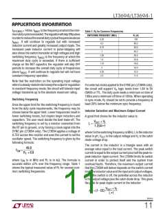
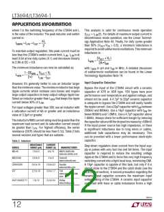
LT3694/LT3694-1
APPLICATIONS INFORMATION
The power section, consisting of the modulator, power
switch and inductor, is modeled as a transconductance
amplifier generating an output current proportional to
capacitor. A 2.5V output presents a special case because it
is marginally adequate to support the boosted drive stage
while using the internal boost diode. For reliable BST pin
operation with 2.5V outputs, use a good external Schottky
diode (such as the ON Semi MBR0540), and a 1μF boost
capacitor (see Figure 4b). For lower output voltages, the
BIAS pin can be tied to the input (Figure 4c), or to another
the voltage at the V pin. Note that the output capacitor
C1
integrates this current, and that the capacitor on the V
C1
pin (C ) integrates the error amplifier output current,
C
resulting in two poles in the loop. In most cases a zero
supply greater than 2.8V. Tying BIAS to V reduces the
is required and comes from either the output capacitor
IN
maximum input voltage to 7V. The circuit in Figure 4a is
more efficient because the BST pin current and BIAS pin
quiescent current comes from a lower voltage source.
One must also ensure that the maximum voltage ratings
of the BST and BIAS pins are not exceeded. The minimum
ESR or from a resistor R in series with C . This simple
C
C
model works well as long as the value of the inductor is
not too high and the loop crossover frequency is much
lower than the switching frequency. A phase lead capaci-
tor (C ) across the feedback divider may improve the
PL
transient response.
V
OUT
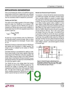
Figure 3 shows the transient response when the load
current steps from 1A to 2.6A and back to 1A.
BIAS BST
LT3694
V
IN
V
IN
C3
SW
GND
4.7µF
V
OUT
100mV/DIV
(4a) For V
> 2.8V
OUT
V
OUT
D2
I
BIAS
BST
L
1A/DIV
V
IN
V
IN
LT3694
C3
SW
36941 F03
GND
4.7µF
100µs/DIV
Figure 3. Transient Load Response of the LT3694
Front Page Application as the Load Current Is
Stepped from 1A to 2.6A. VOUT = 3.3V
(4b) For 2.5V < V
< 2.8V
OUT
BST and BIAS Pin Considerations
V
OUT
BIAS BST
V
CapacitorC3andtheinternalboostSchottkydiode(seethe
Block Diagram in Figure 1) are used to generate a boost
voltage that is higher than the input voltage. In most cases
a 0.22μF capacitor will work well. Figure 4 shows three
ways to arrange the boost circuit. The BST pin must be
more than 2.3V above the SW pin for best efficiency. For
outputs of 3V and above, the standard circuit (Figure 4a)
is best. For outputs between 2.8V and 3V, use a 1μF boost
V
IN
LT3694
IN
C3
SW
GND
4.7µF
36941 FO4
(4c) For V
< 2.5V; V
= 7V
OUT
IN(MAX)
Figure 4. Three Circuits for Generating the Boost Voltage
36941fb
15

 Linear [ Linear ]