LT3694/LT3694-1
APPLICATIONS INFORMATION
Diode Selection
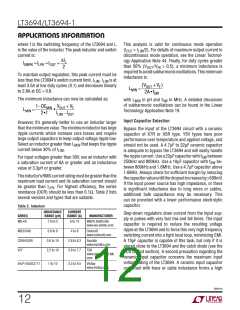
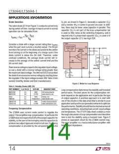
V pin, as shown in Figure 2. Generally a capacitor (C )
C C
and a resistor (R ) in series to ground are used. In addi-
C
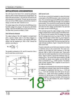
The catch diode (D1 from Figure 1) conducts current only
during switch off time. Average forward current in normal
operation can be calculated from:
tion, there may be lower value capacitor in parallel. This
capacitor (C ) is not part of the loop compensation but
F
is used to filter noise at the switching frequency, and is
VIN − VOUT
required only if a phase-lead capacitor (C ) is used or if
PL
ID(AVG) = IOUT
•
the output capacitor (C1) has high ESR.
VIN
LT3694
Consider a diode with a larger current rating than I
D(AVG)
CURRENT MODE
POWER STAGE
SW
when the part must survive a shorted output. The DA pin
monitors the current in the diode and prevents the switch
from turning on at the beginning of a charge cycle if the
diode current is above the DA limit. Therefore, under
overload conditions, the average diode current will in-
crease to the average of the switch current limit and the
DA current limit.
OUTPUT
ERROR
AMPLIFIER
g
= 7.5S
m
C
PL
R1
FB
–
g
=
m
350µS
ESR
+
0.75V
C1
+
3M
C1
POLYMER
OR
CERAMIC
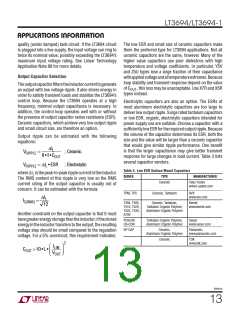
Peakreversevoltageisequaltotheregulatorinputvoltage,
so use a diode with a reverse voltage rating greater than
themaximuminputvoltage.TheinternalOVLOcanprotect
thediodefromexcessivereversevoltagebyshuttingdown
the regulator if the input voltage exceeds 38V. Table 4 lists
several Schottky diodes and their manufacturers.
V
GND
C
TANTALUM
R
C
R2
C
F
C
C
36941 F02
Figure 2. Model for Loop Response
Table 4. Schottky Diodes (40V, 3A)
PART NUMBER
V at 3A (V)
OUTLINE
MANUFACTURER
f
Loop compensation determines the stability and transient
performance. The best values for the compensation net-
work depend on the application and in particular the type
of output capacitor. A practical approach is to start with
one of the circuits in this data sheet that is similar to your
applicationandtunethecompensationnetworktooptimize
theperformance.Stabilityshouldthenbecheckedacrossall
operatingconditions, includingloadcurrent, inputvoltage
and temperature. The LT1375 data sheet contains a more
thorough discussion of loop compensation and describes
how to test the stability using a transient load. Figure 2
shows an equivalent circuit for the LT3694 control loop.
The error amplifier is a transconductance amplifier with
finite output impedance.
MBRS340
MBRD340
0.5
0.6
SMC
D-PAK
ON Semiconductor
www.onsemi.com
B340
SMB340
0.5
0.5
SMC
Diodes, Inc.
Powermite 3 www.diodes.com
CMSH3-40
CSHD3-40
0.5
0.65
SMC
D-PAK
Central Semiconductor
www.centralsemi.com
Frequency Compensation
The LT3694 uses current mode control to regulate the
output.Thissimplifiesloopcompensation.Inparticular,the
LT3694doesnotrequiretheESRoftheoutputcapacitorfor
stability,sotheuserisfreetoemployceramiccapacitorsto
achieve low output ripple and small circuit size. Frequency
compensation is provided by the components tied to the
36941fb
14

 Linear [ Linear ]