LT3694/LT3694-1
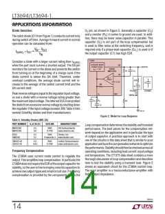
APPLICATIONS INFORMATION
The LDO may be shut down if it is unused by pulling the
FB pin up with a resistor that will source at least 30μA. The
FB pin will clamp at about 1.25V and the LDO will shut off
reducingpowerconsumption.Thispull-upcanbesourced
from one of the LT3694 outputs provided that channel is
always on when the other channels are on.
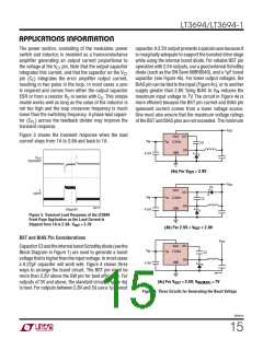
LDO Current Limit
The LDO has a current limit available to reduce the power
consumption of the NPN transistor under overload condi-
tions.ThecurrentlimitrequirestheNPNtransistorcollector
to be connected to the BIAS pin through a low resistance
sense resistor. The current limit circuit senses the voltage
drop across this resistor and reduces the base drive cur-
rent when the limit voltage exceeds 60mV. This will limit
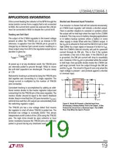
The output stage of the LDO will drive the NPN base from
the BIAS voltage if it is at least 1.8V above the LDO DRIVE
voltage, otherwise the NPN base current comes from V .
the output current to 60mV/R
.
SENSE
IN
The base drive current is limited to 15mA.
If the overload causes the output voltage to drop, the limit
voltage is folded back to reduce power in the NPN transis-
tor. The limit circuit monitors the FB voltage and ramps
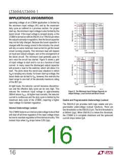
LDO FB Resistor Network
The output voltage of the LDO regulator is programmed
with a resistor divider (refer to the Block Diagram in
Figure 7) between the emitter of the external NPN pass
resistor and the feedback pin, FB2 or FB3. Choose the
resistors according to:
the limit voltage down once V drops to 0.6V. The limit
FB
voltage will fold back to 26mV when V has dropped to
FB
0V. The current foldback is disabled until the associated
TRK/SSpinrisesabove0.68V.Thisinsuresproperstart-up
under full load conditions. Figure 7 shows the LDO circuit
with current limit.
V
0.75
OUT
R1= R2
− 1
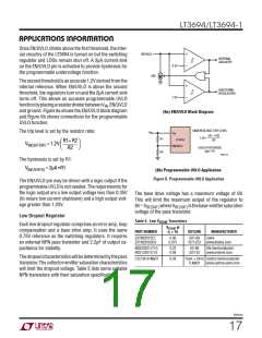
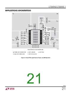
Properlyroutingthecurrentlimitsenseresistorsiscritical
to minimize errors in the current limit. The sense con-
nections are the BIAS pin (both channels) on the high
side and LIM2 or LIM3 on the bottom side. These sense
leads must be routed separately from all current carrying
traces. Figure 9 shows a layout that minimizes trace re-
sistance errors. The current limit sense resistors (RLIM2
and RLIM3) are placed close together and the BIAS pin
The parallel combination of R1 and R2 should be 10k or
less to avoid bias current errors.
OUT1
LT3694
BIAS
60mV
R
SENSE
+
–
trace is connected to V
at their junction. The bottom
OUT1
sides of these resistors have a separate via and trace to
the LIM2 and LIM3 pins.
LIM2
DRV2
Thefoldbackcandramaticallyreducethepowerdissipation
of the NPN pass transistor under short-circuit conditions.
+
–
OUT2
0.75V
For example, an application that has V
= 3.3V and
OUT1
R1
R2
FB2
V
OUT2
= 2.5V will nominally have 0.8V across the pass
transistor V . Under short-circuit conditions, the pass
CE
transistor V will increase to 3.3V. Without foldback the
CE
36941 FO7
power dissipation in the pass transistor will increase by
more than 4x, but with foldback the power dissipation
only increases by 78%.
Figure 7. LDO with Current Limit
36941fb
18

 Linear [ Linear ]