LT3694/LT3694-1
APPLICATIONS INFORMATION
PCB Layout
additional vias to reduce thermal resistance further. With
these steps, the thermal resistance from die (or junction)
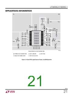
For proper operation and minimum EMI, care must be
taken during printed circuit board layout. Figure 9 shows
the recommended component placement with trace,
ground plane and via locations. Note that large, switched
to ambient can be reduced to θ = 34°C/W (UFD) or
JA
θ =38°C/W(FE20).With100LFPMairflow,thisresistance
JA
can fall by another 25%. Further increases in airflow will
lead to lower thermal resistance.
currents flow in the LT3694’s V , DA, and SW pins, the
IN
BecauseofthelargeoutputcurrentcapabilityoftheLT3694,
it is possible to dissipate enough heat to raise the junc-
tion temperature beyond the absolute maximum. When
operating at high ambient temperatures, the maximum
loadcurrentshouldbederatedastheambienttemperature
catch diode (D1) and the input capacitor (C ). The loop
IN
formed by these components should be as small as pos-
sible. These components, along with the inductor and
output capacitor, should be placed on the same side of
the circuit board, and their connections should be made
on that layer. Place a local, unbroken ground plane below
these components. The SW and BST nodes should be as
approaches T
.
J(MAX)
Power dissipation within the LT3694 can be estimated
by calculating the total power loss from an efficiency
measurement and subtracting the catch diode loss
and inductor loss. The die temperature is calculated by
multiplying the LT3694 power dissipation by the thermal
resistance from junction-to-ambient. Keep in mind other
heat sources—such as the catch diode, inductor and LDO
pass transistors.
small as possible. Finally, keep the FB and V nodes small
C
so that the ground traces will shield them from the SW
and BST nodes.
The exposed pad on the bottom of the package must be
soldered to ground so that the pad acts as a heat sink. To
keep thermal resistance low, extend the top side ground
plane as much as possible, and add thermal vias under
and near the LT3694 to additional ground planes within
the circuit board and on the bottom side.
Other Linear Technology Publications
Application Notes 19, 35 and 44 contain more detailed
descriptions and design information for buck regulators
and other switching regulators. The LT1376 data sheet
has a more extensive discussion of output ripple, loop
compensation and stability testing. Design Note 318
shows how to generate a bipolar output supply using a
buck regulator.
High Temperature Considerations
The PCB must provide heat sinking to keep the LT3694
cool. The Exposed Pad on the bottom of the package must
be soldered to a ground plane. This ground should be tied
to large copper layers below with thermal vias; these lay-
ers will spread the heat dissipated by the LT3694. Place
36941fb
20

 Linear [ Linear ]