LT3694/LT3694-1
APPLICATIONS INFORMATION
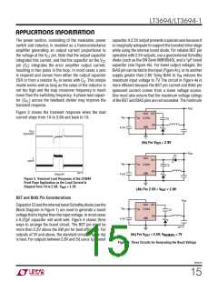
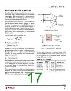
Once EN/UVLO climbs above the first threshold, the inter-
nal circuitry of the LT3694 is turned on but the switching
regulator and LDOs remain shut off. A 2µA current sink
on the EN/UVLO pin is activated to provide hysteresis for
the programmable undervoltage function.
EN/UVLO
+
INTERNAL
CIRCUITRY
0.5V
1.2V
–
2µA
The second threshold is an accurate 1.2V derived from the
internal reference. When EN/UVLO is above the second
threshold, the regulators turn on and the 2µA current sink
turns off. This allows an accurate programmable UVLO
+
SHUTDOWN
REGULATORS
–
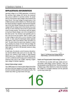
functionbyplacingaresistordividerbetweenV ,EN/UVLO
IN
and ground. Figure 6a shows the EN/UVLO block diagram
and Figure 6b shows connections for the programmable
UVLO function.
(6a) EN/UVLO Block Diagram
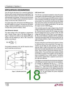
UNDERVOLTAGE TRIP LEVEL
The trip level is set by the resistor ratio:
V
IN
V
IN
(R1 + R2)
R2
1.2V •
R1
R2
LT3694
EN/UVLO
R1+ R2
VIN(UVTRIP) = 1.2V
UVLO HYSTERESIS
R2
2µA • R1
36941 FO4
The hysteresis is set by R1:
VIN(UVHYS) = 2µA •R1
(6b) Programmable UVLO Application
Figure 6. Programmable UVLO Application
The EN/UVLO pin may be driven with a logic output if the
programmable UVLO is not needed. The requirements for
the logic output are a low output voltage less than 0.35V
(to insure low current shutdown) and a high output volt-
age greater than 1.25V.
The base drive voltage has a maximum voltage of 6V.
This will limit the maximum output of the regulator to
6V–V
whereV
isthebase-emittersaturation
BE(SAT)
BE(SAT)
voltage of the pass transistor.
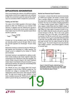
Low Dropout Regulator
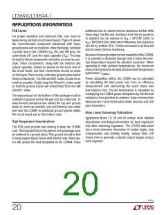
Table 5. Low VCESAT Transistors
Each low dropout regulator comprises an error amp, loop
compensation and a base drive amp. It uses the same
0.75V reference as the switching regulators. It requires
an external NPN pass transistor and 2.2μF of output ca-
pacitance for stability.
V
at
CESAT
C
PART NUMBER
I = 1A
OUTLINE
MANUFACTURER
ZXTN25012EZ
ZXTN25020DG
0.06
0.075
SOT-89
SOT-223
Zetex
www.diodes.com
NSS20201JT1G
NSS12201LT1G
0.22
0.08
SC-89
SOT-23
ON Semiconductor
www.onsemi.com
Thedropoutcharacteristicswillbedeterminedbythepass
transistor. The collector-emitter saturation characteristics
will limit the dropout voltage. Table 5 lists some suitable
NPN transistors with their saturation specifications.
CTLT3410-M621
0.28
Central Semiconductor
www.central-semi.com
1mm × 2mm
TLM621
36941fb
17

 Linear [ Linear ]