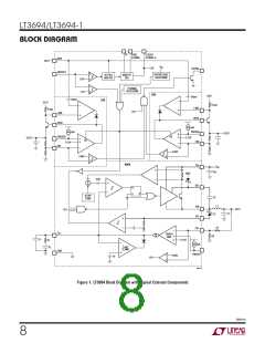
LT3694/LT3694-1
APPLICATIONS INFORMATION
t
=140ns.f
isthefrequencyatwhichthemini-
OFF(MIN)
MAX1
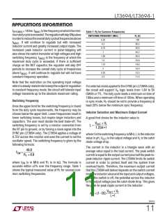
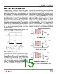
Table 1: RT for Common Frequencies
mumdutycycleisexceeded.TheregulatorwillskipONpulses
inordertoreducetheoveralldutycycleatfrequenciesabove
MAX1
SWITCHING FREQUENCY (MHz)
R (k)
T
0.25
0.5
0.75
1
193
90.2
56.6
40.2
30.5
23.8
19.6
16.0
13.5
11.4
f
. It will continue to regulate but with increased
inductor current and greatly increased output ripple. The
increased peak inductor current in pulse-skipping will
also stress the switch transistor at high voltages and high
1.25
1.5
1.75
2
switching frequency. f
is the frequency at which the
MAX2
maximum duty cycle is exceeded. If there is sufficient
charge on the BST capacitor, the regulator will skip OFF
periods to increase the overall duty cycle at frequencies
2.25
2.5
above f
. It will continue to regulate but will not have
MAX2
constant-frequency operation.
Note that the restriction on the operating input voltage
referstosteady-statelimitstokeeptheoutputinregulation
in constant-frequency mode; the circuit will tolerate input
voltage transients up to the absolute maximum rating.
For external clocks applied to the SYNC pin (LT3694 only),
the circuit will support V logic levels from 1.8V to 5V
H
CMOS or TTL. The duty cycle needs a minimum on time of
100ns and a minimum off time of 100ns. When operating
Switching Frequency
in sync mode, R should be set to provide a frequency at
T
least 20% below the minimum sync frequency.
Once the upper limit for the switching frequency is found
from the duty cycle requirements, the frequency may be
chosen below the upper limit. Lower frequencies result in
lower switching losses, but require larger inductors and
capacitors. The user must decide the best trade-off. The
switching frequency is set by a resistor connected from
the RT pin to ground, or by forcing a clock signal into the
SYNC pin (LT3694 only). The LT3694 applies a voltage of
0.75V across this resistor and uses the current to set the
oscillator speed. The switching frequency is given by the
following formula:
Inductor Selection and Maximum Output Current
A good first choice for the inductor value is:
VOUT + V
1.25A • f
F
L =
wherefistheswitchingfrequencyinMHz,Listheinductor
value in µH, V
is the output voltage and V is the catch
OUT
F
diode voltage drop.
The current in the inductor is a triangle wave with an
average value equal to the load current. The peak switch
current is equalto the outputcurrentplus half thepeak-to-
peak inductor ripple current. The LT3694 limits its switch
current in order to protect itself and the system from
overload faults. Therefore, the maximum output current
that the LT3694 will deliver depends on the switch current
limit, the inductor value and the input and output voltages.
When the switch is off, the potential across the inductor
is the output voltage plus the catch diode drop. This gives
the peak-to-peak ripple current in the inductor:
49.8
RT + 8.8
fSW
=
where f
is in MHz and R is in kΩ. The formula is
SW
T
accurate within 2% over the frequency range. Table 1
shows the typical measured value of R for several com-
T
mon switching frequencies.
VOUT + VF
∆IL = (1− DC)
L • f
36941fb
11

 Linear [ Linear ]