LT3694/LT3694-1
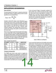
APPLICATIONS INFORMATION
STEP DOWN SWITCHING REGULATOR
each clock cycle if there is sufficient voltage across the
boostcapacitor(C3inFigure 1)tofullysaturatetheoutput
switch. A forced switch off for a minimum time will only
occur at the end of a clock cycle when the boost capaci-
tor needs to be recharged. This operation has the same
effect as lowering the clock frequency for a fixed off time,
resulting in a higher duty cycle and lower minimum input
voltage. The resultant duty cycle depends on the charging
times of the boost capacitor and can be approximated by
the following equation:
Feedback Resistor Network
The output voltage is programmed with a resistor divider
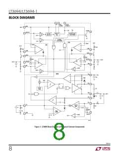
(refertotheBlockDiagraminFigure1)betweentheoutput
and the FB pin. Choose the resistors according to:
VOUT
750mV
R1= R2
− 1
The parallel combination of R1 and R2 should be 10k or
less to avoid bias current errors.
B
B+ 1
DCMAX
=
Input Overvoltage Lockout
where B is the output current divided by the typical
boost current from the BST Pin Current vs Switch Cur-
rent curve in the Typical Performance Characteristics
section.
An important feature of the LT3694 is the ability to survive
transient surges on the input voltage of up to 70V. This is
accomplished by shutting off the regulators to keep this
high voltage off the critical components. The overvoltage
lockout trips when the input voltage exceeds 38V.
Themaximumvoltage, V , forconstant-frequencyopera-
IN
tion is determined by the minimum duty cycle DC
:
MIN
Input Voltage Range
VOUT + VF
DCMIN
Theminimumoperatingvoltageisdeterminedeitherbythe
LT3694’sinternalundervoltagelockoutorbyitsmaximum
duty cycle. The duty cycle is the fraction of time that the
internal switch is on and is determined by the input and
output voltage:
VIN(MAXCF)
=
− VF + VSW
with DC = t
• f
MIN
ON(MIN) SW
Thus, both the maximum and minimum input voltages
for constant-frequency operation are a function of the
switching frequency and output voltage. Therefore, the
maximum switching frequency must be set to a value that
accommodates the input and output voltage parameters
and must meet both of the following criteria:
VOUT + VF
DC=
VIN − VSW + VF
where V is the forward voltage drop of the catch diode
F
and V is the voltage drop of the internal switch (~0.3V
SW
at maximum load). This leads to a minimum input
VOUT + VF
IN(MAXCF) − VSW + V
1
fMAX1
=
•
voltage of:
V
tON(MIN)
F
VOUT + VF
DCMAX(CF)
VIN(MINCF)
=
− VF + VSW
VOUT + VF
VIN(MINCF) − VSW + V
1
fMAX2 = 1−
•
tOFF(MIN)
F
The duty cycle is the fraction of time that the internal
switchisonduringaclockcycle. Themaximumdutycycle
The values of t
SW
ance Characteristics section). Worst-case values for
switchcurrentsgreaterthan0.5Aaret
and t
are functions of
OFF(MIN)
ON(MIN)
for constant-frequency operation given by DC
= 1
I
and temperature (see chart in the Typical Perform-
MAX(CF)
– t
• f . However, unlike most fixed frequency
OFF(MIN)
SW
regulators, the LT3694 will not switch off at the end of
=130nsand
ON(MIN)
36941fb
10

 Linear [ Linear ]