LTC3630
APPLICATIONS INFORMATION
Higher Current Applications
Efficiency Considerations
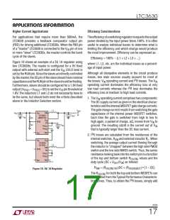
For applications that require more than 500mA, the
LTC3630 provides a feedback comparator output pin
(FBO) for driving additional LTC3630s. When the FBO pin
Theefficiencyofaswitchingregulatorisequaltotheoutput
power divided by the input power times 100%. It is often
useful to analyze individual losses to determine what is
limiting the efficiency and which change would produce
the most improvement. Efficiency can be expressed as:
of a “master” LTC3630 is connected to the V pin of one
FB
or more “slave” LTC3630s, the master controls the burst
cycle of the slaves.
Efficiency = 100% – (L1 + L2 + L3 + ...)
Figure 10 shows an example of a 5V, 1A regulator using
two LTC3630s. The master is configured for a 5V fixed
where L1, L2, etc. are the individual losses as a percent-
age of input power.
output with external soft-start and the V UVLO level is
IN
Although all dissipative elements in the circuit produce
losses, two main sources usually account for most of
set by the RUN pin. Since the slaves are directly controlled
by the master, the SS pin of the slave should have minimal
capacitanceandtheRUNpinoftheslaveshouldbefloating.
Furthermore, slaves should be configured for a 1.8V fixed
2
the losses: V operating current and I R losses. The V
IN
IN
operating current dominates the efficiency loss at very
2
low load currents whereas the I R loss dominates the
output (V
= V = SS) to set the V pin threshold at
PRG2 FB
PRG1
efficiency loss at medium to high load currents.
1.8V. The inductors L1 and L2 do not necessarily have to
be the same, but should both meet the criteria described
above in the Inductor Selection section.
1. The V operating current comprises two components:
IN
The DC supply current as given in the electrical charac-
teristics and the internal MOSFET gate charge currents.
The gate charge current results from switching the gate
capacitance of the internal power MOSFET switches.
Each time the gate is switched from high to low to
L1
V
5V
1A
OUT
V
SW
LTC3630
(MASTER)
V
IN
IN
C
OUT
C
IN
R3
R4
V
SS
FB
RUN
high again, a packet of charge, ΔQ, moves from V to
IN
C
SS
V
PRG1
V
PRG2
ground. The resulting ΔQ/dt is the current out of V
that is typically larger than the DC bias current.
IN
I
FBO
SET
2
2. I R losses are calculated from the resistances of the
internal switches, R and external inductor R . When
SW
L
V
V
FB
IN
LTC3630
(SLAVE)
switching, the average output current flowing through
the inductor is “chopped” between the high side PMOS
switch and the low side NMOS switch. Thus, the series
resistance looking back into the switch pin is a function
L2
SW
SS
RUN
V
PRG1
V
PRG2
of the top and bottom switch R
values and the
DS(ON)
I
FBO
SET
3630 F10
duty cycle (DC = V /V ) as follows:
OUT IN
R
= (R )DC + (R
DS(ON)TOP
) • (1 – DC)
DS(ON)BOT
SW
Figure 10. 5V, 1A Regulator
The R
for both the top and bottom MOSFETs can
DS(ON)
be obtained from the Typical Performance Characteris-
2
tics curves. Thus, to obtain the I R losses, simply add
3630fb
17

 Linear Systems [ Linear Systems ]