LTC3630
APPLICATIONS INFORMATION
R
SW
to R and multiply the result by the square of the
For the MSOP package the θ is 45°C/W. Thus, the junc-
L
JA
average output current:
tion temperature of the regulator is:
2
2
I R Loss = I (R + R )
45°C
W
O
SW
L
TJ = 85°C+0.475W •
= 106.4°C
Other losses, including C and C
ESR dissipative
IN
OUT
losses and inductor core losses, generally account for
which is below the maximum junction temperature of
150°C.
less than 2% of the total power loss.
NotethatthewhiletheLTC3630isindropout,itcanprovide
output current that is equal to the peak current of the part.
This can increase the chip power dissipation dramatically
and may cause the internal overtemperature protection
circuitry to trigger at 180°C and shut down the LTC3630.
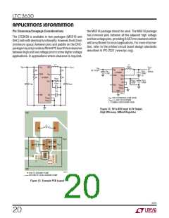
Thermal Considerations
Inmostapplications,theLTC3630doesnotdissipatemuch
heat due to its high efficiency. But, in applications where
the LTC3630 is running at high ambient temperature with
low supply voltage and high duty cycles, such as dropout,
the heat dissipated may exceed the maximum junction
temperature of the part.
Design Example
As a design example, consider using the LTC3630 in an
To prevent the LTC3630 from exceeding the maximum
junctiontemperature,theuserwillneedtodosomethermal
analysis. The goal of the thermal analysis is to determine
whetherthepowerdissipatedexceedsthemaximumjunc-
tion temperature of the part. The temperature rise from
ambient to junction is given by:
application with the following specifications: V = 24V,
IN
V
= 70V, V
= 3.3V, I
= 500mA, f = 200kHz.
Furthermore, assume for this example that switching
IN(MAX)
OUT
OUT
should start when V is greater than 12V.
IN
First, calculate the inductor value that gives the required
switching frequency:
T = P • θ
JA
R
D
⎛
⎜
⎝
⎞ ⎛
⎠ ⎝
⎞
⎟
⎠
3.3V
200kHz •1.2A
3.3V
24V
L =
• 1–
≅ 10ꢀH
requirement.
⎟ ⎜
where P is the power dissipated by the regulator and θ
D
JA
is the thermal resistance from the junction of the die to
the ambient temperature.
Next, verify that this value meets the L
MIN
For this input voltage and peak current, the minimum
inductor value is:
The junction temperature is given by:
T = T + T
R
J
A
24V •150ns
LMIN
=
≅ 3ꢀH
Generally, the worst-case power dissipation is in dropout
at low input voltage. In dropout, the LTC3630 can provide
a DC current as high as the full 1.2A peak current to the
output. At low input voltage, this current flows through a
higher resistance MOSFET, which dissipates more power.
1.2A
Therefore, the minimum inductor requirement is satisfied
and the 10μH inductor value may be used.
Next,C andC
areselected.Forthisdesign,C should
IN
IN
OUT
be sized for a current rating of at least:
Asanexample,considertheLTC3630indropoutataninput
voltage of 5V, a load current of 500mA and an ambient
temperatureof85°C.FromtheTypicalPerformancegraphs
3.3V
24V
24V
3.3V
IRMS = 500mA •
•
– 1≅ 175mARMS
of Switch On-Resistance, the R
of the top switch
DS(ON)
at V = 5V and 100°C is approximately 1.9Ω. Therefore,
IN
the power dissipated by the part is:
2
2
P = (I
) • R
= (500mA) • 1.9Ω = 0.475W
DS(ON)
D
LOAD
3630fb
18

 Linear Systems [ Linear Systems ]