LTC3630
APPLICATIONS INFORMATION
Pin Clearance/Creepage Considerations
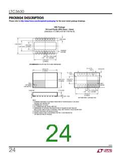
the MSE16 package should be used. The MSE16 package
has removed pins between all the adjacent high voltage
andlowvoltagepins,providing0.657mmclearancewhich
will be sufficient for most applications. For more informa-
tion, refer to the printed circuit board design standards
described in IPC-2221 (www.ipc.org).
The LTC3630 is available in two packages (MSE16 and
DHC)bothwithidenticalfunctionality.However,the0.2mm
(minimum space) between pins and paddle on the DHC-
packagemaynotprovidesufficientPCboardtraceclearance
between high and low voltage pins in some higher voltage
applications. In applications where clearance is required,
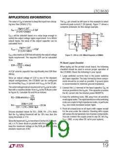
L1
L1
V
IN
V
33ꢀH
V
V
SW
OUT
IN
OUT
5V
V
IN
V
SW
LTC3630
IN
5V TO 65V
R3
R4
R1
R2
C
C
OUT
IN
500mA
100ꢀF
4.7ꢀF
V
RUN
FB
RUN
V
w2
FB
LTC3630
R
C
ISET
I
SET
SS
C
R
ISET
ISET
I
SET
100pF
220k
ISET
C
IN
C
OUT
FBO
V
V
PRG1
PRG2
GND
C
SS
3630 F13
FBO
SS
V
PRG2
V
PRG1
C
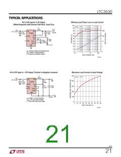
: TDK C5750X7R2A-475M (2220)
OUT
IN
C
: 2 wꢀAVX 1812D107MAT
L1: SUMIDA CDRH105RNP-330N
Figure 13. 5V to 65V Input to 5V Output,
High Efficiency, 500mA Regulator
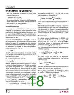
GND
L1
V
OUT
C
IN
C
OUT
V
IN
GND
VIAS TO GROUND PLANE
3630 F12
OUTLINE OF LOCAL GROUND PLANE
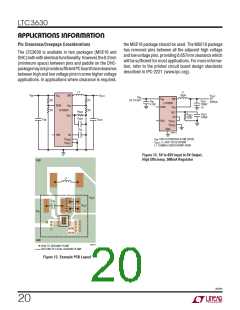
Figure 12. Example PCB Layout
3630fb
20

 Linear Systems [ Linear Systems ]