LTC3630
APPLICATIONS INFORMATION
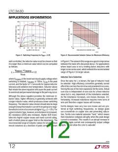
Different core materials and shapes will change the size/
currentandprice/currentrelationshipofaninductor.Toroid
or shielded pot cores in ferrite or permalloy materials are
small and do not radiate energy but generally cost more
than powdered iron core inductors with similar charac-
teristics. The choice of which style inductor to use mainly
depends on the price versus size requirements and any
radiated field/EMI requirements. New designs for surface
mount inductors are available from Coiltronics, Coilcraft,
TDK, Toko, and Sumida.
or choose a capacitor rated at a higher temperature than
required.Severalcapacitorsmayalsobeparalleledtomeet
size or height requirements in the design.
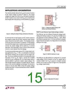
The output capacitor, C , filters the inductor’s ripple
OUT
current and stores energy to satisfy the load current when
the LTC3630 is in sleep. The output ripple has a lower limit
of V /160 due to the 5mV typical hysteresis of the feed-
OUT
back comparator. The time delay of the comparator adds
an additional ripple voltage that is a function of the load
current. During this delay time, the LTC3630 continues to
switch and supply current to the output. The output ripple
can be approximated by:
C and C
Selection
IN
OUT
The input capacitor, C , is needed to filter the trapezoidal
IN
IPEAK
2
4 •10–6 VOUT
⎛
⎜
⎝
⎞
⎟
⎠
current at the source of the top high side MOSFET. C
IN
ΔVOUT
≈
–ILOAD
•
+
COUT
160
should be sized to provide the energy required to charge
the inductor without causing a large decrease in input
Theoutputrippleisamaximumatnoloadandapproaches
lower limit of V /160 at full load. Choose the output
voltage (ΔV ). The relationship between C and ΔV
IN
IN
IN
OUT
is given by:
capacitor C
to limit the output voltage ripple ΔV
OUT
OUT
2
L •IPEAK
using the following equation:
CIN >
2 • V • ΔV
IN
IN
–6
I
• 2 • 10
V
PEAK
C
≥
OUT
It is recommended to use a larger value for C than
OUT
IN
ΔV
–
OUT
calculated by the above equation since capacitance de-
160
creases with applied voltage. In general, a 4.7ꢀF X7R
The value of the output capacitor must be large enough
to accept the energy stored in the inductor without a large
change in output voltage during a single switching cycle.
ceramiccapacitorisagoodchoiceforC inmostLTC3630
IN
applications.
To minimize large ripple voltage, a low ESR input capaci-
tor sized for the maximum RMS current should be used.
RMS current is given by:
Setting this voltage step equal to 1% of the output voltage,
the output capacitor must be:
2
⎛
⎞
I
VOUT
V
IN
V
IN
VOUT
PEAK
C
> 50 • L •
IRMS =IOUT(MAX)
•
•
– 1
⎜
⎝
⎟
⎠
OUT
V
OUT
Typically, a capacitor that satisfies the voltage ripple re-
quirementisadequatetofiltertheinductorripple. Toavoid
overheating, the output capacitor must also be sized to
handle the ripple current generated by the inductor. The
worst-case ripple current in the output capacitor is given
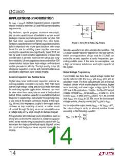
This formula has a maximum at V = 2V , where I =
RMS
OUT
fordesignbecauseevensignificantdeviationsdonotoffer
muchrelief.Notethatripplecurrentratingsfromcapacitor
manufacturers are often based only on 2000 hours of life
which makes it advisable to further derate the capacitor,
IN
OUT
I
/2.Thissimpleworst-caseconditioniscommonlyused
3630fb
13

 Linear Systems [ Linear Systems ]