LTC3630
APPLICATIONS INFORMATION
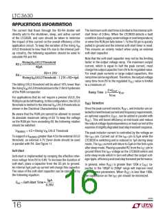
The value of C is selected to keep the input from droop-
The I pin should be left open in this example to select
IN
SET
ing less than 240mV (1%):
maximum peak current (1.2A typical). Figure 11 shows a
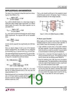
complete schematic for this design example.
10ꢀH•1.2A2
2 • 24V • 240mV
will be selected based on a value large enough to
CIN >
≅ 2.2ꢀF
10ꢀH
V
OUT
V
IN
3.3V
V
SW
LTC3630
IN
24V
C
OUT
500mA
200k
satisfy the output voltage ripple requirement. For a 50mV
output ripple, the value of the output capacitor can be
calculated from:
V
FB
RUN
FBO
SS
47ꢀF
2.2ꢀF
4.7V
V
V
PRG2
21k
PRG1
I
SET
10ꢀH•1.2A2
2 • 3.3V • 50mV
GND
COUT
>
≅ 47ꢀF
3630 F11
C
also needs an ESR that will satisfy the output voltage
Figure 11. 24V to 3.3V, 500mA Regulator at 200kHz
OUT
ripple requirement. The required ESR can be calculated
from:
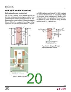
PC Board Layout Checklist
50mV
1.2A
ESR <
≅ 40mΩ
When laying out the printed circuit board, the following
checklist should be used to ensure proper operation of
the LTC3630. Check the following in your layout:
A 47ꢀF ceramic capacitor has significantly less ESR than
40mΩ.
1. Large switched currents flow in the power switches
and input capacitor. The loop formed by these compo-
nents should be as small as possible. A ground plane
is recommended to minimize ground impedance.
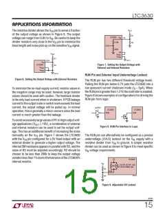
Since an output voltage of 3.3V is one of the standard
output configurations, the LTC3630 can be configured
by connecting V
to ground and V
to the SS pin.
PRG1
PRG2
TheundervoltagelockoutrequirementonV canbesatis-
IN
2. Connect the (+) terminal of the input capacitor, C , as
IN
fied with a resistive divider from V to the RUN pin (refer
IN
close as possible to the V pin. This capacitor provides
IN
to Figure 9). Calculate R3 and R4 as follows:
the AC current into the internal power MOSFETs.
12V
40ꢀA
3. Keep the switching node, SW, away from all sensitive
smallsignalnodes.Therapidtransitionsontheswitching
node can couple to high impedance nodes, in particular
R3 = 200kwhichis ≤
200k •1.21V
12V – 1.21V+200k • 4ꢀA
V , and create increased output ripple.
R4 =
= 20.9k
FB
4. Flood all unused area on all layers with copper except
for the area under the inductor. Flooding with copper
will reduce the temperature rise of power components.
Choose standard values for R3 = 200k, R4 = 21k. Note
that the V falling threshold will be 10% less than the
IN
You can connect the copper areas to any DC net (V ,
rising threshold or 11V.
IN
V
OUT
, GND, or any other DC rail in your system).
SincethemaximumV ismorethan4.5xtheUVLOthresh-
IN
old, a 4.7V Zener diode in parallel with R4 is required to
keep the maximum voltage on the RUN pin less than the
absolute maximum of 6V.
3630fb
19

 Linear Systems [ Linear Systems ]