LTC3630
(Refer to Block Diagram)
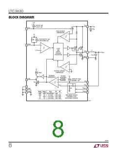
OPERATION
The LTC3630 is a synchronous step-down DC/DC con-
verter with internal power switches that uses Burst Mode
control. The low quiescent current and high switching
frequency results in high efficiency across a wide range
of load currents. Burst Mode operation functions by using
short“burst”cyclestoswitchtheinductorcurrentthrough
the internal power MOSFETs, followed by a sleep cycle
where the power switches are off and the load current is
supplied by the output capacitor. During the sleep cycle,
the LTC3630 draws only 12ꢀA of supply current. At light
loads, the burst cycles are a small percentage of the total
cycle time which minimizes the average supply current,
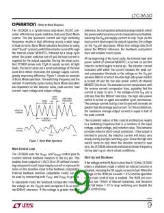
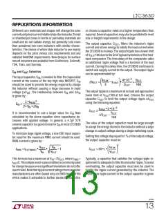
greatly improving efficiency. Figure 1 shows an example
of Burst Mode operation. The switching frequency and the
number of switching cycles during Burst Mode operation
are dependent on the inductor value, peak current, load
current, input voltage and output voltage.
reference,thecomparatoractivatesasleepmodeinwhich
thepowerswitchesandcurrentcomparatorsaredisabled,
reducing the V pin supply current to only 12ꢀA. As the
IN
load current discharges the output capacitor, the voltage
on the V pin decreases. When this voltage falls 5mV
FB
below the 800mV reference, the feedback comparator
trips and enables burst cycles.
At the beginning of the burst cycle, the internal high side
power switch (P-channel MOSFET) is turned on and the
inductor current begins to ramp up. The inductor current
increases until either the current exceeds the peak cur-
rent comparator threshold or the voltage on the V pin
FB
exceeds 800mV, at which time the high side power switch
is turned off and the low side power switch (N-channel
MOSFET)turnson. Theinductorcurrentrampsdownuntil
the reverse current comparator trips, signaling that the
current is close to zero. If the voltage on the V pin is
FB
still less than the 800mV reference, the high side power
switch is turned on again and another cycle commences.
The average current during a burst cycle will normally be
greaterthantheaverageloadcurrent.Forthisarchitecture,
the maximum average output current is equal to half of
the peak current.
SLEEP
SWITCHING
FREQUENCY
CYCLE
BURST
CYCLE
INDUCTOR
CURRENT
BURST
FREQUENCY
The hysteretic nature of this control architecture results
in a switching frequency that is a function of the input
voltage, output voltage, and inductor value. This behavior
provides inherent short-circuit protection. If the output is
shorted to ground, the inductor current will decay very
slowly during a single switching cycle. Since the high side
switch turns on only when the inductor current is near
zero,theLTC3630inherentlyswitchesatalowerfrequency
during start-up or short-circuit conditions.
OUTPUT
VOLTAGE
ΔV
3630 F01
OUT
Figure 1. Burst Mode Operation
Main Control Loop
The LTC3630 uses the V
and V
control pins to
PRG1
PRG2
Start-Up and Shutdown
connect internal feedback resistors to the V pin. This
FB
enables fixed outputs of 1.8V, 3.3V or 5V without increas-
ing component count, input supply current or exposure to
noise on the sensitive input to the feedback comparator.
External feedback resistors (adjustable mode) can still
IfthevoltageontheRUNpinislessthan0.7V, theLTC3630
enters a shutdown mode in which all internal circuitry is
disabled,reducingtheDCsupplycurrentto5ꢀA.Whenthe
voltage on the RUN pin exceeds 1.21V, normal operation
of the main control loop is enabled. The RUN pin com-
parator has 110mV of internal hysteresis, and therefore
must fall below 1.1V to stop switching and disable the
main control loop.
be used by connecting both V
and V
to ground.
PRG1
PRG2
In adjustable mode the feedback comparator monitors
the voltage on the V pin and compares it to an inter-
FB
nal 800mV reference. If this voltage is greater than the
3630fb
9

 Linear Systems [ Linear Systems ]