iCE40 HX-Series Ultra-Low Power Family
AC Timing Guidelines
The following examples provide some guidelines of device performance. The actual performance depends on the
specific application and how it is physically implemented in the iCE40 FPGA using the Lattice iCEcube2 software.
The following guidelines assume typical conditions (VCC = 1.0 V or 1.2 V as specified, temperature = 25 ˚C). Apply
derating factors using the iCEcube2 timing analyzer to adjust to other operating regimes.
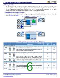
Programmable Logic Block (PLB) Timing
Table 8 provides timing information for the logic in a Programmable Logic Block (PLB), which includes the paths
shown in Figure 5 and Figure 6.
Figure 5 PLB Sequential Timing Circuit
PAD
PIO
DFF
PAD
PIO
D
Q
LUT4
Logic Cell
Logic Cell
GBIN
PAD
GBUF
Figure 6 PLB Combinational Timing Circuit
PAD
PIO
PIO
LUT4
Logic Cell
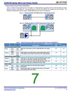
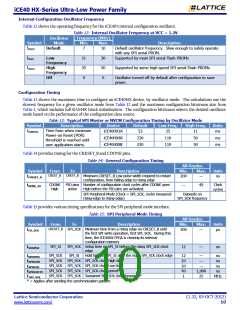
Table 8: Typical Programmable Logic Block (PLB) Timing
Nominal VCC
1.2 V
Typ.
Description
units
MHz
ns
Sequential Logic Paths
Flip-flop toggle frequency. DFF flip-flop output fed back to LUT4 input with
4-input XOR, clocked on same clock edge
FTOGGLE
GBIN
input
DFF
GBIN
input
PIO
256
3.9
Logic cell flip-flop (DFF) clock-to-output time, measured from the DFF CLK
input to PIO output, including interconnect delay.
tCKO
clock
input
GBIN
input
output
Global Buffer Input (GBIN) delay, though Global Buffer (GBUF) clock network
to clock input on the logic cell DFF flip-flop.
tGBCKLC
DFF
clock
input
GBIN
input
PIO
1.5
ns
Minimum setup time on PIO input, through LUT4, to DFF flip-flop D-input
before active clock edge on the GBIN input, including interconnect delay.
tSULI
tHDLI
PIO
.67
0
ns
ns
input
GBIN
input
Minimum hold time on PIO input, through LUT4, to DFF flip-flop D-input
after active clock edge on the GBIN input, including interconnect delay.
input
Combinational Logic Paths
Asynchronous delay from PIO input pad to adjacent PLB interconnect.
tLUT4IN
PIO
LUT4
input
LUT4
output
PIO
1.8
0.34
3.7
ns
ns
ns
input
LUT4
input
LUT4
Logic cell LUT4 combinational logic propagation delay, regardless of logic
complexity from input to output.
tILO
Asynchronous delay from adjacent PLB interconnect to PIO output
pad.
tLUT4IN
output output
Lattice Semiconductor Corporation
(1.32, 03-OCT-2012)
www.latticesemi.com/
6

 LATTICE [ LATTICE SEMICONDUCTOR ]