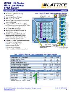
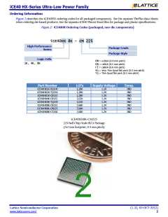
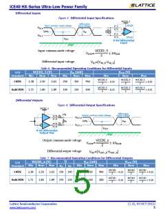
iCE40 HX-Series Ultra-Low Power Family
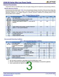
Electrical Characteristics
All parameter limits are specified under worst-case supply voltage, junction temperature, and processing conditions.
Absolute Maximum Ratings
Stresses beyond those listed under Table 2 may cause permanent damage to the device. These are stress ratings only;
functional operation of the device at these or any other conditions beyond those listed under the Recommended
Operating Conditions is not implied. Exposure to absolute maximum conditions for extended periods of time
adversely affects device reliability.
Table 2: Absolute Maximum Ratings
Symbol
Description
Minimum Maximum
Units
VCC
VPP_2V5
VPP_FAST
VCCIO_0
VCCIO_1
VCCIO_2
VCCIO_3
SPI_VCC
VIN_0
Core supply Voltage
–0.5
1.42
V
V
V
V
VPP_2V5 NVCM programming and operating supply
Optional fast NVCM programming supply
I/O bank supply voltage (I/O Banks 0, 1, 2 and 3 plus SPI
interface)
–0.5
4.00
Voltage applied to PIO pin within a specific I/O bank (I/O
Banks 0, 1, 2 and 3 plus SPI interface)
–1.0
3.6
V
VIN_1
VIN_2
VIN_SPI
VIN_3
VCCPLL
IOUT
TJ
TSTG
Analog voltage supply to the Phase Locked Loop (PLL)
DC output current per pin
Junction temperature
–0.5
—
–55
–65
1.30
20
125
150
V
mA
°C
°C
Storage temperature, no bias
Recommended Operating Conditions
Table 3: Recommended Operating Conditions
Minimum Nominal Maximum Units
Symbol
VCC
Description
High Performance, low-power
Core supply voltage
VPP_2V5 NVCM
1.14
1.30
2.30
2.30
1.20
—
—
1.26
3.47
3.47
3.00
V
V
V
V
VPP_2V51
Release from Power-on Reset
Configure from NVCM
NVCM programming
programming and operating
supply
—
VPP_FAST2
SPI_VCC
VCCIO_0
VCCIO_1
VCCIO_2
VCCIO_3
SPI_VCC
VCCPLL3
TA
Optional fast NVCM programming supply
SPI interface supply voltage
Leave unconnected in application
1.71
2.70
2.38
—
3.30
2.50
3.47
3.47
2.63
V
V
V
I/O standards, all banks
LVCMOS33
LVCMOS25, LVDS
LVCMOS18, SubLVDS
LVCMOS15
1.71
1.43
1.80
1.50
1.89
1.58
V
V
Analog voltage supply to the Phase Locked Loop (PLL)
Ambient temperature
NVCM programming temperature
1.14
–40
10
1.20
—
25
1.26
85
30
V
°C
°C
TPROG
Notes:
1. VPP_2V5 must be connected to a valid voltage, when the iCE40HX device is active.
2. VPP_FAST, used only for fast production programming, must be left floating or unconnected in application.
3. VCCPLL must be tied to VCC when PLL is not used.
Lattice Semiconductor Corporation
(1.32, 03-OCT-2012)
www.latticesemi.com/
3

 LATTICE [ LATTICE SEMICONDUCTOR ]