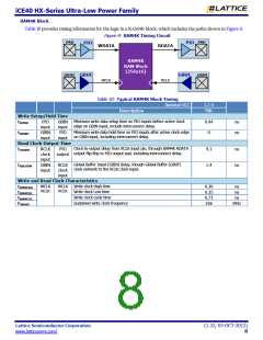
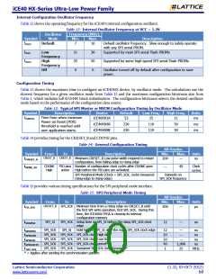
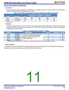
iCE40 HX-Series Ultra-Low Power Family
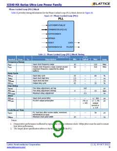
Phase-Locked Loop (PLL) Block
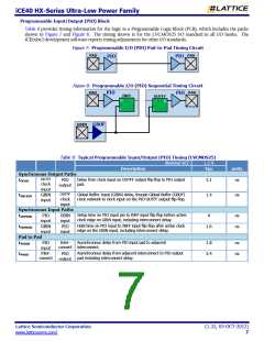
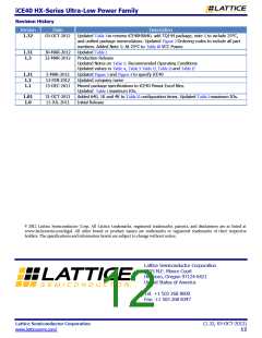
Table 11 provides timing information for the Phase-Locked Loop (PLL) block shown in Figure 10.
Figure 10: Phase-Locked Loop (PLL)
PLL
LATCHINPUTVALUE
DYNAMICDELAY[3:0]
EXTFEEDBACK
BYPASS
RESET
LOCK
REFERENCECLK
PLLOUT
Table 11: Phase-Locked Loop (PLL) Block Timing
Nominal VCC 1.2 V
Min.
Typical
Max.
Symbol From
Frequency Range
FREF
To
Description
Units
Input clock frequency range
10
16
—
—
133
533
MHz
MHz
Output clock frequency range (cannot exceed
maximum frequency supported by global
buffers)
FOUT
Duty Cycle
PLLIJ
TwHI
TwLOW
PLLOJ
Input duty cycle
35
2.5
2.5
45
—
—
—
—
65
—
—
55
%
ns
ns
%
Input clock high time
Input clock low time
Output duty cycle
Fine Delay
tFDTAP
PLLTAPS
PLLFDAM
Jitter
Fine delay adjustment, per tap
Fine delay adjustment settings
Maximum delay adjustment
165
—
2.5
ps
taps
ns
0
15
Input clock period jitter
PLLOUT output period jitter
PLLIPJ
PLLOPJ
—
—
—
1% or
≤ 100
+/- 300
+/- 1.1%
output
ps
ps
period or
≥ꢐ110
Lock/Reset Time
tLOCK
PLL lock time after receive stable, monotonic
REFERENCECLK input
Minimum reset pulse width
—
—
—
50
μs
twRST
20
—
ns
Notes:
1. Output jitter performance is affected by input jitter. A clean reference clock < 100ps jitter must be used to ensure
best jitter performance.
2. The output jitter specification refers to the intrinsic jitter of the PLL.
Lattice Semiconductor Corporation
(1.32, 03-OCT-2012)
www.latticesemi.com/
9

 LATTICE [ LATTICE SEMICONDUCTOR ]