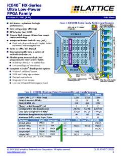
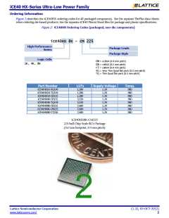
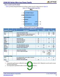
iCE40 HX-Series Ultra-Low Power Family
I/O Characteristics
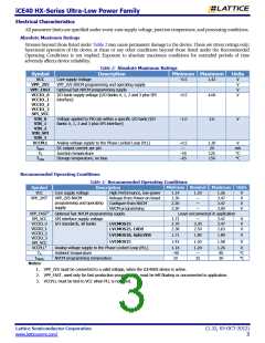
Table 4: PIO Pin Electrical Characteristics
Symbol
Description
Conditions
Minimum
Nominal
Maximum
±10
Units
µA
µA
Il
IOZ
Input pin leakage current VIN = VCCIOmax to 0 V
Three-state I/O pin (Hi-Z) VO = VCCIOmax to 0 V
leakage current
±10
CPIO
CGBIN
PIO pin input capacitance
GBIN global buffer pin
6
6
pF
pF
input capacitance
RPULLUP Internal PIO pull-up
resistance during
VCCIO = 3.3V
VCCIO = 2.5V
VCCIO = 1.8V
60
80
120
160
50
kΩ
kΩ
kΩ
kΩ
mV
configuration
VCCIO = 1.5V
VHYST
Input hysteresis
VCCIO = 1.5V to 3.3V
NOTE: All characteristics are characterized and may or may not be tested on each pin on each device.
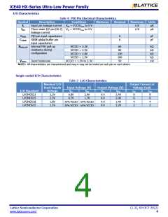
Single-ended I/O Characteristics
Table 5: I/O Characteristics
Nominal I/O
Output Current at
Voltage (mA)
Bank Supply
Voltage
3.3V
Input Voltage (V)
Output Voltage (V)
I/O Standard
LVCMOS33
LVCMOS25
LVCMOS18
LVCMOS15
IOH
VIL
VIH
VOL
0.4
0.4
0.4
0.4
VOH
2.40
2.00
1.40
1.20
IOL
0.80
0.70
2.00
1.70
8
8
2.5V
1.8V
1.5V
6
6
4
4
35% VCCIO 65% VCCIO
35% VCCIO 65% VCCIO
2
2
Lattice Semiconductor Corporation
(1.32, 03-OCT-2012)
www.latticesemi.com/
4

 LATTICE [ LATTICE SEMICONDUCTOR ]