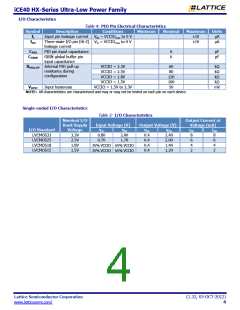
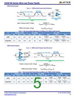
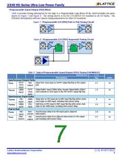
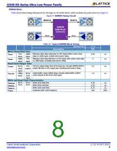
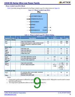
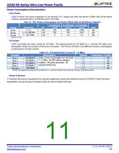
iCE40 HX-Series Ultra-Low Power Family
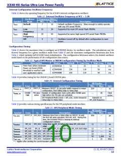
Internal Configuration Oscillator Frequency
Table 12 shows the operating frequency for the iCE40’s internal configuration oscillator.
Table 12: Internal Oscillator Frequency at VCC = 1.2V
Frequency (MHz)
Oscillator
Mode
Symbol
fOSCD
Min.
Max.
Description
Default oscillator frequency. Slow enough to safely operate
with any SPI serial PROM.
Default
7
10
fOSCL
fOSCH
Low
Frequency
High
Frequency
Off
21
35
0
30
50
0
Supported by most SPI serial Flash PROMs
Supported by some high-speed SPI serial Flash PROMs
Oscillator turned off by default after configuration to save
power.
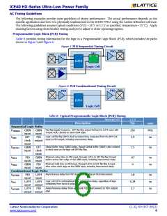
Configuration Timing
Table 13 shows the maximum time to configure an iCE40HX device, by oscillator mode. The calculations use the
slowest frequency for a given oscillator mode from Table 12 and the maximum configuration bitstream size from
Table 1, which includes full RAM4K block initialization. The configuration bitstream selects the desired oscillator
mode based on the performance of the configuration data source.
Table 13: Typical SPI Master or NVCM Configuration Timing by Oscillator Mode
Symbol
tCONFIGL
Description
Time from when minimum
Power-on Reset (POR)
threshold is reached until
user application starts.
Device
iCE40HX1K
Default
Low Freq.
High Freq.
Units
ms
53
25
11
iCE40HX4K
iCE40HX8K
230
230
110
110
50
50
ms
ms
Table 14 provides timing for the CRESET_B and CDONE pins.
Table 14: General Configuration Timing
All Grades
Symbol
tCRESET_B
From
CREST_B
To
CREST_B
Description
Minimum CRESET_B Low pulse width required to restart
configuration, from falling edge to rising edge
Min.
200
Max.
—
Units
ns
CDONE
High
PIO pins Number of configuration clock cycles after CDONE goes
Clock
cycles
tDONE_IO
—
49
active
High before the PIO pins are activated.
SPI Peripheral Mode (Clock = SPI_SCK, cycles measured
rising-edge to rising-edge)
Depends on
SPI_SCK frequency
Table 15 provides various timing specifications for the SPI peripheral mode interface.
Table 15: SPI Peripheral Mode Timing
All Grades
Symbol
tCR_SCK
From
CRESET_B
To
Description
Min.
300
Max.
—
Units
µs
SPI_SCK Minimum time from a rising edge on CRESET_B until
the first SPI write operation, first SPI_SCK. During this
time, the iCE40HX FPGA is clearing its internal
configuration memory
SPI_SI
SPI_SCK Setup time on SPI_SI before the rising SPI_SCK clock
edge
tSUSPISI
12
—
ns
SPI_SCK
SPI_SI
Hold time on SPI_SI after the rising SPI_SCK clock edge
tHDSPISI
tSPISCKH
tSPISCKL
tSPISCKCYC
FSPI_SCK
12
20
20
40
1
—
—
—
1,000
25
ns
ns
ns
ns
MHz
SPI_SCK SPI_SCK SPI_SCK clock High time
SPI_SCK SPI_SCK SPI_SCK clock Low time
SPI_SCK SPI_SCK SPI_SCK clock period*
SPI_SCK SPI_SCK Sustained SPI_SCK clock frequency*
* = Applies after sending the synchronization pattern.
Lattice Semiconductor Corporation
(1.32, 03-OCT-2012)
www.latticesemi.com/
10

 LATTICE [ LATTICE SEMICONDUCTOR ]