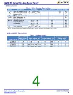
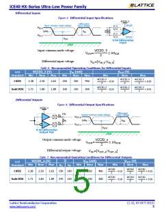
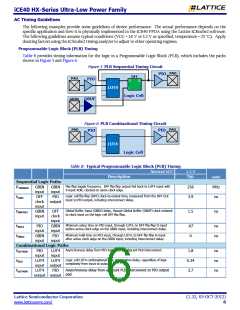
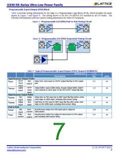
iCE40 HX-Series Ultra-Low Power Family
RAM4K Block
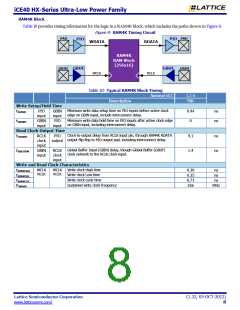
Table 10 provides timing information for the logic in a RAM4K block, which includes the paths shown in Figure 9.
Figure 9: RAM4K Timing Circuit
PAD
PAD
PIO
PIO
WDATA
RDATA
RAM4K
RAM Block
(256x16)
GBIN
GBIN
GBUF
GBUF
WCLK
RCLK
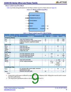
Table 10: Typical RAM4K Block Timing
Nominal VCC
1.2 V
Typ.
Description
Write Setup/Hold Time
Minimum write data setup time on PIO inputs before active clock
edge on GBIN input, include interconnect delay.
tSUWD
PIO
GBIN
input
PIO
input
0.44
0
ns
ns
input
GBIN
input
Minimum write data hold time on PIO inputs after active clock edge
on GBIN input, including interconnect delay.
tHDWD
Read Clock-Output-Time
Clock-to-output delay from RCLK input pin, through RAM4K RDATA
output flip-flop to PIO output pad, including interconnect delay.
tCKORD
RCLK
clock
input
GBIN
input
PIO
output
4.1
1.4
ns
ns
Global Buffer Input (GBIN) delay, though Global Buffer (GBUF)
clock network to the RCLK clock input.
tGBCKRM
RCLK
clock
input
Write and Read Clock Characteristics
WCLK
RCLK
WCLK
RCLK
Write clock High time
Write clock Low time
Write clock cycle time
Sustained write clock frequency
tRMWCKH
tRMWCKL
tRMWCYC
FWMAX
0.30
0.35
0.71
256
ns
ns
ns
MHz
Lattice Semiconductor Corporation
(1.32, 03-OCT-2012)
www.latticesemi.com/
8

 LATTICE [ LATTICE SEMICONDUCTOR ]