X5043, X5045
the array that is block lock protected can be read but not
written. It will remain protected until the BL bits are altered to
disable block lock protection of that portion of memory.
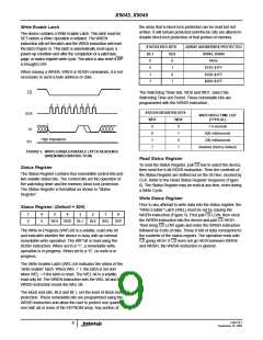
Write Enable Latch
The device contains a Write Enable Latch. This latch must be
SET before a Write Operation is initiated. The WREN
instruction will set the latch and the WRDI instruction will reset
the latch (Figure 5). This latch is automatically reset upon a
power-up condition and after the completion of a valid byte,
page, or status register write cycle. The latch is also reset if WP
is brought LOW.
STATUS REG BITS
ARRAY ADDRESSES PROTECTED
BL1
0
BL0
0
X5043, X5045
None
0
1
$180–$1FF
$100–$1FF
$000–$1FF
When issuing a WREN, WRDI or RDSR commands, it is not
necessary to send a byte address or data.
1
0
1
1
CS
The Watchdog Timer bits, WD0 and WD1, select the
Watchdog Time-out Period. These nonvolatile bits are
programmed with the WRSR instruction.
0
1
2
3
4
5
6
7
STATUS REGISTER BITS
WATCHDOG TIME OUT
SCK
WD1
WD0
(TYPICAL)
1.4 seconds
0
0
1
1
0
1
0
1
SI
600 milliseconds
200 milliseconds
disabled (factory default)
High Impedance
SO
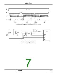
FIGURE 5. WRITE ENABLE/DISABLE LATCH SEQUENCE
(WREN/WRDI INSTRUCTION)
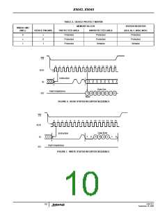
Read Status Register
To read the Status Register, pull CS low to select the device,
then send the 8-bit RDSR instruction. Then the contents of
the Status Register are shifted out on the SO line, clocked by
CLK. Refer to the Read Status Register Sequence (Figure
6). The Status Register may be read at any time, even during
a Write Cycle.
Status Register
The Status Register contains four nonvolatile control bits and
two volatile status bits. The control bits set the operation of
the watchdog timer and the memory block lock protection.
The Status Register is formatted as shown in “Status
Register”.
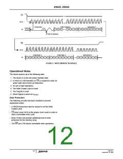
Write Status Register
Prior to any attempt to write data into the status register, the
“Write Enable” Latch (WEL) must be set by issuing the
WREN instruction (Figure 5). First pull CS LOW, then clock
the WREN instruction into the device and pull CS HIGH.
Then bring CS LOW again and enter the WRSR instruction
followed by 8 bits of data. These 8 bits of data correspond to
the contents of the status register. The operation ends with
CS going HIGH. If CS does not go HIGH between WREN
and WRSR, the WRSR instruction is ignored.
Status Register: (Default = 30H)
7
6
5
4
3
2
1
0
0
0
WD1 WD0
BL1
BL0
WEL
WIP
The Write-In-Progress (WIP) bit is a volatile, read only bit
and indicates whether the device is busy with an internal
nonvolatile write operation. The WIP bit is read using the
RDSR instruction. When set to a “1”, a nonvolatile write
operation is in progress. When set to a “0”, no write is in
progress.
The Write Enable Latch (WEL) bit indicates the status of the
“write enable” latch. When WEL = 1, the latch is set and
when WEL = 0 the latch is reset. The WEL bit is a volatile,
read only bit. The WREN instruction sets the WEL bit and the
WRDS instruction resets the WEL bit.
The block lock bits, BL0 and BL1, set the level of block lock
protection. These nonvolatile bits are programmed using the
WRSR instruction and allow the user to protect one quarter,
one half, all or none of the EEPROM array. Any portion of
FN8126.1
9
September 16, 2005

 INTERSIL [ Intersil ]