X5043, X5045
SPI Serial Memory
The memory portion of the device is a CMOS Serial
EEPROM array with Intersil’s block lock protection. The array
is internally organized as 512 x 8 bits. The device features a
Serial Peripheral Interface (SPI) and software protocol
allowing operation on a simple four-wire bus.
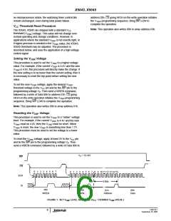
VTRIP Programming
Execute
Reset VTRIP
Sequence
The device utilizes Intersil’s proprietary Direct Write™ cell,
providing a minimum endurance of 1,000,000 cycles and a
minimum data retention of 100 years.
Set VCC = VCC Applied =
Desired VTRIP
The device is designed to interface directly with the
synchronous Serial Peripheral Interface (SPI) of many
popular microcontroller families.
New VCC Applied
New VCC Applied
Execute
Set VTRIP
Sequence
=
=
Old VCC Applied
Old VCC Applied
- Error
- Error
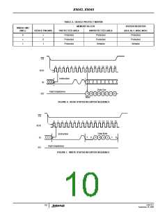
The device contains an 8-bit instruction register that controls
the operation of the device. The instruction code is written to
the device via the SI input. There are two write operations
that requires only the instruction byte. There are two read
operations that use the instruction byte to initiate the output
of data. The remainder of the operations require an
instruction byte, an 8-bit address, then data bytes. All
instruction, address and data bits are clocked by the SCK
input. All instructions (Table 1), addresses and data are
transferred MSB first.
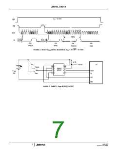
Apply 5V to VCC
Execute
Reset VTRIP
Sequence
Decrement VCC
(VCC = VCC–10mV)
NO
RESET pin
goes active?
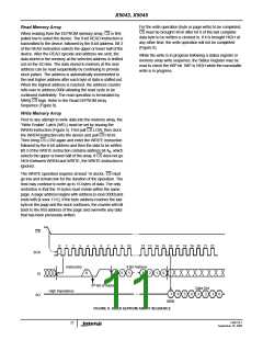
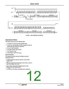
Clock and Data Timing
YES
Data input on the SI line is latched on the first rising edge of
SCK after CS goes LOW. Data is output on the SO line by
the falling edge of SCK. SCK is static, allowing the user to
stop the clock and then start it again to resume operations
where left off. CS must be LOW during the entire operation.
Measured VTRIP
-Desired VTRIP
Error ≤ -Emax
Error ≥ Emax
-Emax < Error < Emax
DONE
Emax = Maximum Desired Error
FIGURE 4. VTRIP PROGRAMMING SEQUENCE
TABLE 1. INSTRUCTION SET
INSTRUCTION NAME
INSTRUCTION FORMAT*
0000 0110
OPERATION
Set the Write Enable Latch (Enable Write Operations)
Reset the Write Enable Latch (Disable Write Operations)
Read Status Register
WREN
WRDI
0000 0100
RSDR
WRSR
READ
WRITE
0000 0101
0000 0001
Write Status Register (Watchdog and Block Lock)
Read Data from Memory Array Beginning at Selected Address
Write Data to Memory Array Beginning at Selected Address (1 to 16 bytes)
0000 A8011
0000 A8010
Note: *Instructions are shown MSB in leftmost position. Instructions are transferred MSB first.
FN8126.1
8
September 16, 2005

 INTERSIL [ Intersil ]