X5043, X5045
For the write operation (byte or page write) to be completed,
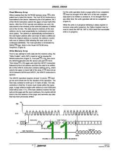
Read Memory Array
CS must be brought HIGH after bit 0 of the last complete
data byte to be written is clocked in. If it is brought HIGH at
any other time, the write operation will not be completed
(Figure 9).
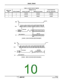
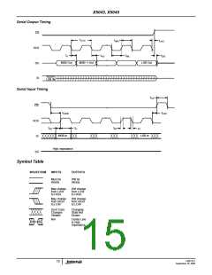
When reading from the EEPROM memory array, CS is first
pulled low to select the device. The 8-bit READ instruction is
transmitted to the device, followed by the 8-bit address. Bit 3
of the READ instruction selects the upper or lower half of the
device. After the READ opcode and address are sent, the
data stored in the memory at the selected address is shifted
out on the SO line. The data stored in memory at the next
address can be read sequentially by continuing to provide
clock pulses. The address is automatically incremented to
the next higher address after each byte of data is shifted out.
When the highest address is reached, the address counter
rolls over to address 000h allowing the read cycle to be
continued indefinitely. The read operation is terminated by
taking CS high. Refer to the Read EEPROM Array
While the write is in progress following a status register or
memory array write sequence, the Status Register may be
read to check the WIP bit. WIP is HIGH while the nonvolatile
write is in progress.
Sequence (Figure 8).
Write Memory Array
Prior to any attempt to write data into the memory array, the
“Write Enable” Latch (WEL) must be set by issuing the
WREN instruction (Figure 5). First pull CS LOW, then clock
the WREN instruction into the device and pull CS HIGH.
Then bring CS LOW again and enter the WRITE instruction
followed by the 8-bit address and then the data to be written.
Bit 3 of the WRITE instruction contains address bit A8, which
selects the upper or lower half of the array. If CS does not go
HIGH between WREN and WRITE, the WRITE instruction is
ignored.
The WRITE operation requires at least 16 clocks. CS must
go low and remain low for the duration of the operation. The
host may continue to write up to 16 bytes of data. The only
restriction is that the 16 bytes must reside within the same
page. A page address begins with address [x xxxx 0000] and
ends with [x xxxx 1111]. If the byte address reaches the last
byte on the page and the clock continues, the counter will roll
back to the first address of the page and overwrite any data
that has been previously written.
CS
0
1
2
3
4
5
6
7
8
9
6
10
12 13 14 15 16 17 18 19 20 21 22
SCK
SI
Instruction
8 Bit Address
7
5
3
2
1
0
8
9th Bit of Address
Data Out
High Impedance
7
6
5
4
3
2
1
0
SO
MSB
FIGURE 8. READ EEPROM ARRAY SEQUENCE
FN8126.1
September 16, 2005
11

 INTERSIL [ Intersil ]