X5043, X5045
cycle has already been initiated, WP going low will have no
affect on a write.
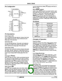
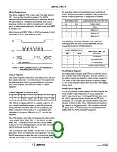
Pin Configuration
8 Ld SOIC/PDIP/MSOP
Reset (RESET, RESET)
X5043, X5045, RESET/RESET is an active low/HIGH, open
drain output which goes active whenever VCC falls below the
minimum VCC sense level. It will remain active until VCC
rises above the minimum VCC sense level for 200ms.
RESET/RESET also goes active if the Watchdog timer is
enabled and CS remains either high or low longer than the
Watchdog time out period. A falling edge of CS will reset the
watchdog timer.
V
1
8
CS/WDI
SO
CC
2
3
4
7
6
5
RESET/RESET
X5043, X5045
WP
SCK
SI
V
SS
14 Ld TSSOP
1
V
14
CS
SO
NC
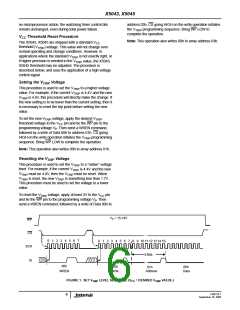
Pin Names
CC
2
3
4
5
6
7
13
12
RESET/RESET
SYMBOL
DESCRIPTION
Chip Select Input
Serial Output
NC
NC
CS/WDI
X5043, X5045
11
10
9
NC
NC
SO
NC
SCK
SI
SI
SCK
Serial Input
WP
Serial Clock Input
Write Protect Input
Ground
V
8
SS
WP
VSS
Pin Descriptions
Serial Output (SO)
VCC
Supply Voltage
Reset Output
RESET/RESET
SO is a push/pull serial data output pin. During a read cycle,
data is shifted out on this pin. Data is clocked out by the
falling edge of the serial clock.
Principles of Operation
Power-on Reset
Serial Input (SI)
Application of power to the X5043, X5045 activate a Power-
on Reset Circuit. This circuit pulls the RESET/RESET pin
active. RESET/RESET prevents the system microprocessor
from starting to operate with insufficient voltage or prior to
stabilization of the oscillator. When VCC exceeds the device
SI is the serial data input pin. All opcodes, byte addresses,
and data to be written to the memory are input on this pin.
Data is latched by the rising edge of the serial clock.
Serial Clock (SCK)
VTRIP value for 200ms (nominal) the circuit releases
The Serial Clock controls the serial bus timing for data input
and output. Opcodes, addresses, or data present on the SI
pin is latched on the rising edge of the clock input, while data
on the SO pin changes after the falling edge of the clock
input.
RESET/RESET, allowing the processor to begin executing
code.
Low Voltage Monitoring
During operation, the X5043, X5045 monitor the VCC level
and asserts RESET/RESET if supply voltage falls below a
preset minimum VTRIP. The RESET/RESET signal prevents
the microprocessor from operating in a power fail or
brownout condition. The RESET/RESET signal remains
active until the voltage drops below 1V. It also remains active
until VCC returns and exceeds VTRIP for 200ms.
Chip Select (CS/WDI)
When CS is high, the X5043, X5045 are deselected and the
SO output pin is at high impedance and, unless an internal
write operation is underway, the X5043, X5045 will be in the
standby power mode. CS low enables the X5043, X5045,
placing it in the active power mode. It should be noted that
after power-up, a high to low transition on CS is required prior
to the start of any operation.
Watchdog Timer
The Watchdog Timer circuit monitors the microprocessor
activity by monitoring the WDI input. The microprocessor
must toggle the CS/WDI pin periodically to prevent an active
RESET/RESET signal. The CS/WDI pin must be toggled
from HIGH to LOW prior to the expiration of the watchdog
time out period. The state of two nonvolatile control bits in
the Status Register determines the watchdog timer period.
The microprocessor can change these watchdog bits. With
Write Protect (WP)
When WP is low, nonvolatile writes to the X5043, X5045 are
disabled, but the part otherwise functions normally. When
WP is held high, all functions, including non volatile writes
operate normally. WP going low while CS is still low will
interrupt a write to the X5043, X5045. If the internal write
FN8126.1
5
September 16, 2005

 INTERSIL [ Intersil ]