X5043, X5045
Absolute Maximum Ratings
Recommended Operating Conditions
Temperature:
Temperature under bias. . . . . . . . . . . . . . . . . . . . . .-65°C to +135°C
Storage temperature . . . . . . . . . . . . . . . . . . . . . . . .-65°C to +150°C
Voltage on any pin with
respect to VSS . . . . . . . . . . . . . . . . . . . . . . . . . . . . . . . .-1.0V to +7V
D.C. output current. . . . . . . . . . . . . . . . . . . . . . . . . . . . . . . . . . . 5mA
Lead temperature (soldering, 10 seconds) . . . . . . . . . . . . . . .300°C
Commercial. . . . . . . . . . . . . . . . . . . . . . . . . . . . . . . . 0°C to +70°C
Industrial . . . . . . . . . . . . . . . . . . . . . . . . . . . . . . . . .-40°C to +85°C
Supply Voltage:
-2.7, -2.7A . . . . . . . . . . . . . . . . . . . . . . . . . . . . . . . . . 2.7V to 5.5V
Blank, -4.5A . . . . . . . . . . . . . . . . . . . . . . . . . . . . . . . . 4.5V to 5.5V
CAUTION: Stresses above those listed under “Absolute Maximum Ratings” may cause permanent damage to the device. This is a stress rating only; functional
operation of the device (at these or any other conditions above those listed in the operational sections of this specification) is not implied. Exposure to absolute
maximum rating conditions for extended periods may affect device reliability.
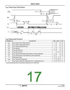
DC Electrical Specifications (Over the recommended operating conditions unless otherwise specified.)
LIMITS
SYMBOL
ICC1
PARAMETER
VCC Write Current (Active)
VCC Read Current (Active)
TEST CONDITIONS/COMMENTS
SCK = 3.3MHz(3); SO, RESET, RESET = Open
MIN
TYP(2)
MAX
UNIT
mA
3
2
ICC2
SCK = 3.3MHz(3); SI = VSS, RESET, RESET =
Open
mA
ISB1
ISB2
ILI
VCC Standby Current WDT = OFF CS = VCC, SCK, SI = VSS, VCC = 5.5V
VCC Standby Current WDT = ON CS = VCC, SCK, SI = VSS, VCC = 5.5V
10
50
µA
µA
µA
µA
V
Input Leakage Current
Output Leakage Current
Input LOW Voltage
SCK, SI, WP = VSS to VCC
SO, RESET, RESET = VSS to VCC
SCK, SI, WP, CS
0.1
0.1
10
ILO
10
(1)
VIL
-0.5
VCC x 0.3
VCC + 0.5
0.4
(1)
VIH
Input HIGH Voltage
SCK, SI, WP, CS
VCC x 0.7
V
VOL
Output LOW Voltage (SO)
IOL = 2mA @ VCC = 2.7V
V
I
OL = 0.5mA @ VCC = 1.8V
VOH1
VOH2
VOH3
VOLRS
Output HIGH Voltage (SO)
Output HIGH Voltage (SO)
Output HIGH Voltage (SO)
VCC > 3.3V, IOH = –1.0mA
VCC - 0.8
VCC - 0.4
VCC - 0.2
V
V
V
V
2V < VCC ≤ 3.3V, IOH = –0.4mA
V
CC ≤ 2V, IOH = –0.25mA
Output LOW Voltage (RESET,
RESET)
IOL = 1mA
0.4
Capacitance TA = +25°C, f = 1MHz, VCC = 5V
SYMBOL
TEST
Output Capacitance (SO, RESET, RESET)
Input Capacitance (SCK, SI, CS, WP)
CONDITIONS
MAX
UNIT
(2)
COUT
VOUT = 0V
VIN = 0V
8
6
pF
pF
(2)
CIN
NOTES:
1. VIL min. and VIH max. are for reference only and are not tested.
2. This parameter is periodically sampled and not 100% tested.
3. SCK frequency measured from VCC x 0.1/VCC x 0.9
FN8126.1
13
September 16, 2005

 INTERSIL [ Intersil ]