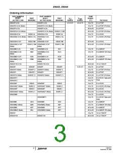
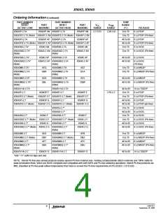
X5043, X5045
no microprocessor action, the watchdog timer control bits
remain unchanged, even during total power failure.
address 03h. CS going HIGH on the write operation initiates
the VTRIP programming sequence. Bring WP LOW to
complete the operation.
V
Threshold Reset Procedure
CC
Note: This operation also writes 00h to array address 03h.
The X5043, X5045 are shipped with a standard VCC
threshold (VTRIP) voltage. This value will not change over
normal operating and storage conditions. However, in
applications where the standard VTRIP is not exactly right, or
if higher precision is needed in the VTRIP value, the X5043,
X5045 threshold may be adjusted. The procedure is
described below, and uses the application of a high voltage
control signal.
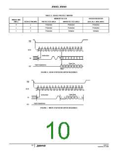
Setting the V
Voltage
TRIP
This procedure is used to set the VTRIP to a higher voltage
value. For example, if the current VTRIP is 4.4V and the new
V
TRIP is 4.6V, this procedure will directly make the change. If
the new setting is to be lower than the current setting, then it
is necessary to reset the trip point before setting the new
value.
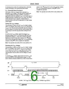
To set the new VTRIP voltage, apply the desired VTRIP
threshold voltage to the VCC pin and tie the WP pin to the
programming voltage VP. Then send a WREN command,
followed by a write of Data 00h to address 01h. CS going
HIGH on the write operation initiates the VTRIP programming
sequence. Bring WP LOW to complete the operation.
Note: This operation also writes 00h to array address 01h.
Resetting the V
Voltage
TRIP
This procedure is used to set the VTRIP to a “native” voltage
level. For example, if the current VTRIP is 4.4V and the new
V
TRIP must be 4.0V, then the VTRIP must be reset. When
TRIP is reset, the new VTRIP is something less than 1.7V.
V
This procedure must be used to set the voltage to a lower
value.
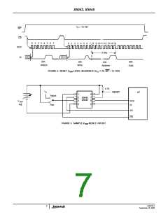
To reset the VTRIP voltage, apply at least 3V to the VCC pin
and tie the WP pin to the programming voltage VP. Then
send a WREN command, followed by a write of Data 00h to
VP = 15-18V
WP
CS
0
1 2 3 4 5 6 7
0
1
2 3
4
5 6 7 8 9 10 11 12 13 14 15
SCK
8 Bits
SI
06h
02h
00h
01h
WREN
Write
Address
Data
FIGURE 1. SET VTRIP LEVEL SEQUENCE (VCC = DESIRED VTRIP VALUE.)
FN8126.1
6
September 16, 2005

 INTERSIL [ Intersil ]