ISL6753
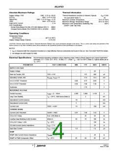
Absolute Maximum Ratings
Thermal Information
Thermal Resistance Junction to Ambient (Typical)
16 Lead QSOP (Note 1). . . . . . . . . . . . . . . . . . . . . .
Maximum Junction Temperature . . . . . . . . . . . . . . . .-55°C to 150°C
Maximum Storage Temperature Range. . . . . . . . . . .-65°C to 150°C
Maximum Lead Temperature (Soldering 10s) . . . . . . . . . . . . . 300°C
(QSOP- Lead Tips Only)
Supply Voltage, VDD . . . . . . . . . . . . . . . . . . . GND - 0.3V to +20.0V
θ
(°C/W)
95
JA
OUTxxx . . . . . . . . . . . . . . . . . . . . . . . . . . . . . . . GND - 0.3V to VDD
Signal Pins. . . . . . . . . . . . . . . . . . . . . . . GND - 0.3V to V
+ 0.3V
REF
VREF . . . . . . . . . . . . . . . . . . . . . . . . . . . . . . . . . GND - 0.3V to 6.0V
Peak GATE Current . . . . . . . . . . . . . . . . . . . . . . . . . . . . . . . . . . 0.1A
ESD Classification
Human Body Model (Per MIL-STD-883 Method 3015.7) . . .3000V
Charged Device Model (Per EOS/ESD DS5.3, 4/14/93) . . .1000V
Operating Conditions
Temperature Range
ISL6753AAxx . . . . . . . . . . . . . . . . . . . . . . . . . . .-40°C to 105°C
Supply Voltage Range (Typical). . . . . . . . . . . . . . . . . . . . 9-16 VDC
CAUTION: Stresses above those listed in “Absolute Maximum Ratings” may cause permanent damage to the device. This is a stress only rating and operation of the
device at these or any other conditions above those indicated in the operational sections of this specification is not implied.
NOTES:
1. θ is measured with the component mounted on a high effective thermal conductivity test board in free air. See Tech Brief TB379 for details.
JA
2. All voltages are with respect to GND.
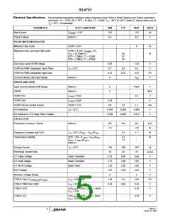
Electrical Specifications Recommended operating conditions unless otherwise noted. Refer to Block Diagram and Typical Application
schematic. 9 V < VDD< 20 V, RTD = 10.0kΩ, CT = 470pF, T = -40°C to 105°C (Note 3), Typical values are at
A
T
= 25°C
A
PARAMETER
SUPPLY VOLTAGE
TEST CONDITIONS
MIN
TYP
MAX
UNITS
Supply Voltage
-
-
20
400
15.5
9.00
7.50
-
-
µA
mA
V
Start-Up Current, IDD
Operating Current, IDD
UVLO START Threshold
UVLO STOP Threshold
Hysteresis
VDD = 5.0V
, C
-
-
175
11.0
8.75
7.00
1.75
R
= 0
LOAD OUT
8.00
6.50
-
V
V
REFERENCE VOLTAGE
Overall Accuracy
I
= 0 - -10mA
4.850
-
5.000
5.150
V
VREF
Long Term Stability
Operational Current (source)
Operational Current (sink)
Current Limit
T
= 125°C, 1000 hours (Note 4)
3
-
-
mV
mA
mA
mA
A
-10
5
-
-
-
VREF = 4.85V
-15
-
-100
CURRENT SENSE
Current Limit Threshold
CS to OUT Delay
VERR = VREF
Excl. LEB (Note 4)
(Note 4)
0.97
1.00
1.03
50
V
ns
ns
ns
Ω
-
50
-
35
70
-
Leading Edge Blanking (LEB) Duration
CS to OUT Delay + LEB
100
130
20
T
= 25°C
A
CS Sink Current Device Impedance
Input Bias Current
V
V
= 1.1V
= 0.3V
-
-
CS
CS
-1.0
-
1.0
µA
RAMP
RAMP Sink Current Device Impedance
RAMP to PWM Comparator Offset
V
= 1.1V
-
-
20
95
Ω
RAMP
T
= 25°C
65
80
mV
A
FN9182.1
March 10, 2005
4

 INTERSIL [ Intersil ]