ISL6366
Powering Up And Open-Loop Test Voltage-Regulator (VR) Design
Materials
The ISL6366 features very easy debugging and powering up. For
the first-time powering up, an open-loop test can be done by
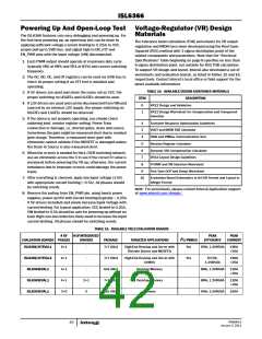
The tolerance band calculation (TOB) worksheets for VR output
applying sufficient voltage (current limiting to 0.25A) to VCC,
regulation and IMON have been developed using the Root-Sum-
proper pull-up to SVID bus, and signal high to EN_VTT and
Squared (RSS) method with 3 sigma distribution point of the
EN_PWR pins with the input voltage (VIN) disconnected.
related components and parameters. Note that the “Electrical
Specifications” table beginning on page 8 specifies no less than
1. Each PWM output should operate at maximum duty cycle
6 sigma distribution point, not suitable for RSS TOB calculation.
(typically VR0 at 98% and VR1 at 83%) and correct switching
To support VR design and layout, Intersil also developed a set of
frequency.
worksheets and evaluation boards, as listed in Tables 15 and 16,
2. The 0C, 0D, 0E, and 0F registers can be read via SVID bus to
respectively. Contact Intersil’s local office or field support for the
check its proper setting if an VTT tool is installed and
latest available information.
operating.
TABLE 15. AVAILABLE DESIGN ASSISTANCE MATERIALS
3. If 5V drivers are used and share the same rail as VCC, the
proper switching on UGATEs and LGATEs should be seen.
ITEM
DESCRIPTION
VR12 Design and Validation
4. If 12V drivers are used and can be disconnected from VIN and
sourced by an external 12V supply, the proper switching on
UGATEs and LGATEs should be observed.
0
1
VR12 Design Worksheet for Compensation and Component
Selection
5. If the above is not properly operating, you should check
soldering joint, resistor register setting, Power Train
connection or damage, i.e, shorted gates, drain and source.
Sometimes the gate might be measured short due to residual
gate charge. Therefore, a measured short gate with
ohmmeter cannot validate if the MOSFET is damaged unless
the Drain to Source is also measured short.
2
3
Transient Response Optimization Guidelines
VOUT and IMON TOB Calculator
4
SVID and PMBus Communication Tool
Resistor Register Calculator
5
6
Dynamic VID Compensation Calculator
VR12 Layout Design Guidelines
6. When the re-work is needed for the L/DCR matching network,
use an ohmmeter across the C to see if the correct R value is
measured before powering the VR up; otherwise, the current
imbalance due to improper re-work could damage the power
trains.
7
8
TCOMP and TM Selection Worksheet
Fine Tune OCP and Droop Worksheet
9
7. After everything is checked, apply low input voltage (1-5V)
with appropriate current limiting (~0.5A). All phases should
be switching evenly.
10
Evaluation Board Schematics in OrCAD Format and Layout in
Allegro Format
NOTE: For worksheets, please contact Intersil Application support
at www.intersil.com/design/.
8. Remove the pull-up from EN_PWR pin, using bench power
supplies, power up VCC with current limiting (typically ~ 0.25A
if 5V drivers included) and slowly increase Input Voltage with
current limiting. For typical application, VCC limited to 0.25A,
VIN limited to 0.5A should be safe for powering up without no
load. High core-loss inductors likely need to increase the input
current limiting. All phases should be switching evenly.
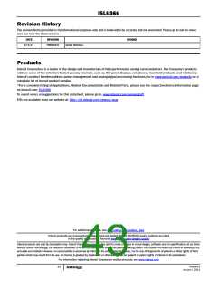
TABLE 16. AVAILABLE VR12 EVALUATION BOARDS
# OF
#OFINTEGRATED
PEAK
EFFICIENCY
PEAK
CURRENT
2
EVALUATION BOARDS PHASES
DRIVERS
-
PACKAGE
7x7 60Ld
TARGETED APPLICATIONS
I C/PMBUS
ISL6366/67EVAL1
ISL6366/67EVAL2
ISL6364EVAL1
6+1
6+1
4+1
4+1
3+0
High-End Desktop and Server with
Discrete Drivers and MOSFETs
Yes
93%, 1.2V@50A
190A
+25A
-
-
7x7 60Ld
6x6 48Ld
7x7 60Ld
5x5 40Ld
High-End Desktop and Server with
DrMOS
Yes
93.5%,
1.2V@50A
190A
+25A
Desktop/Memory
Desktop/Memory
Memory
88%, 1.2V@50A
88%, 1.2V@50A
94%, 1.5V@25A
120A
+35A
ISL6363EVAL1
2+1
2
120A
+35A
ISL6353EVAL1
100A
FN6964.0
January 3, 2011
42

 INTERSIL [ Intersil ]