ISL6366
VCC
TM
TM
Thermal Trip
Point Lookup
Table (90-1200C)
40.98%*VCC
39.12%*VCC
RTM
TMAX
+
VR_HOT#
RNTC1
oc
VR_HOT#
-
RTMS
TMS
+
-
TEMPERATURE
T1
T2
RNTC2
oc
ISL6366
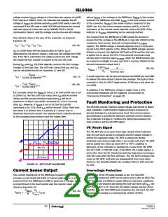
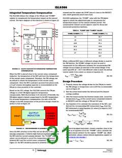
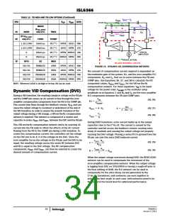
FIGURE 21. VR_HOT# SIGNAL (TMAX = 100°C) vs TM VOLTAGE
NTC BETA ~ 3477
Based on the NTC temperature characteristics and the desired
threshold of the VR_HOT# signal, the pull-up resistor R of TM
pin is given by Equation 21:
TM
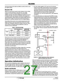
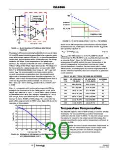
FIGURE 19. BLOCK DIAGRAM OF THERMAL MONITORING
FUNCTION
R
= 1.557xR
NTC(T2)
(EQ. 21)
TM
The diagram of thermal monitoring function block is shown in Figure
19. One NTC resistor should be placed close to the respective power
stage of the voltage regulator VR0 and VR1 to sense the operational
temperature, and one pull-up resistor is needed to form the voltage
divider for the TM pin. As the temperature of the power stage
increases, the resistance of the NTC will reduce, resulting in the
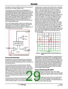
reduced voltage at the TM pin. Figure 20 shows the TM voltage over
the temperature for a typical design with a recommended 6.8kΩ
NTC (P/N: NTHS0805N02N6801 from Vishay, β = 3477) and 1kΩ
R
is the NTC resistance at the VR_HOT# threshold
NTC(T2)
temperature T2. The VR_HOT# is de-asserted at temperature T1,
as shown in Table 7. Since the NTC directly senses the
temperature of the PCB and not the exact temperature of the
hottest component on the board due to airflow and varied
thermal impedance, therefore, the user should select a lower
TMAX number, depending upon the mismatching between NTC
and the hottest components, than such component to guarantee
a safe operation.
resistor R . It is recommended to use those resistors for the
TM
accurate temperature compensation since the internal thermal
digital code is developed based upon these two components. If a
different value is used, the temperature coefficient must be close to
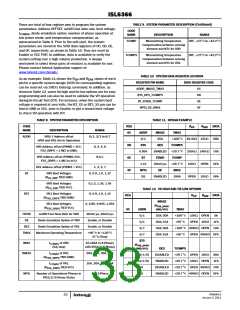
TABLE 7. VR_HOT# TYPICAL TRIP POINT AND HYSTERESIS
TMAX
(°C)
VR_HOT# LOW (°C;
T2, %VCC)
VR_HOT# OPEN
(°C; T1, %VCC)
HYSTERESIS
(°C)
3477 and R must be scaled accordingly. For instance, say
TM
NTC = 10kΩ (β = 3477), then R should be 10kΩ/6.8kΩ*1kΩ =
TM
90
88.6; 45.52%
94.3; 42.26%
100.0; 39.12%
106.1; 36.14%
109.1; 33.32%
115.5; 30.68%
118.7; 28.24%
85.9; 47.56%
91.4; 44.20%
97.1; 40.98%
103.0; 37.92%
106.1; 35.00%
112.3; 32.24%
115.5; 29.7%
2.7
2.9
2.9
3.1
3.0
3.2
3.2
1.47kΩ.
95
There is a comparator with hysteresis to compare the TM pin
voltage to the threshold set by the TMAX register for VR_HOT#
signal. With TMAX set at +100°C, the VR_HOT# signal is pulled
to GND when either TM or TMS voltage is lower than 39.12% of
VCC voltage, and is open when both TM and TMS voltages
increase to above 40.98% of VCC voltage. The comparator trip
point will be programmable by TMAX values. Figure 20 shows the
operation of those signals.
100
105
110
115
120
100
90
80
70
60
50
40
30
20
Temperature Compensation
The ISL6366 supports inductor DCR sensing, or resistive sensing
techniques. The inductor DCR has a positive temperature
coefficient, which is about +0.385%/°C. Since the voltage across
the inductor is sensed for the output current information, the
sensed current has the same positive temperature coefficient as
the inductor DCR.
In order to obtain the correct current information, there should be
a way to correct the temperature impact on the current sense
component. ISL6366 provides two methods: integrated
temperature compensation and external temperature
compensation.
0
20
40
60
80
100
120
140
o
TEMPERATURE ( C)
FIGURE 20. THE RATIO OF TM VOLTAGE TO NTC TEMPERATURE
WITH RECOMMENDED PARTS
FN6964.0
January 3, 2011
30

 INTERSIL [ Intersil ]