ISL6366
The CPU can enter four distinct power states as shown in Table 2.
The VR1 output can be disabled by pulling PWMS to VCC while the
respective address is released for use with a different VR controller.
For proper operation of VR0, the VR1’s respective pins should be
configured as described in “Disabling Output” on page 35.
The ISL6366 supports all states, but it treats PSI2 and PSI3 the
same. In addition, the setDecay mode will automatically enter PSI2
State while decaying the output voltage. However, prior to the end of
soft-start (i.e: VR_RDY goes high), the lower power mode
(PSI1/2/3/Decay) is NOT enabled.
While the controller is operational (VCC above POR, EN_VTT and
EN_PWR are both high, valid VID inputs), it can pull the PWM pins
to ~40% of VCC (~2V for 5V VCC bias) during various stages, such
as soft-start delay, phase shedding operation, or fault conditions
(OC or OV events). The matching driver's internal PWM resistor
divider can further raise the PWM potential, but not lower it
below the level set by the controller IC. Therefore, the controller's
PWM outputs are directly compatible with Intersil drivers that
require 5V PWM signal amplitudes. Drivers requiring 3.3V PWM
signal amplitudes are generally incompatible.
TABLE 2. POWER STATE COMMAND FROM CPU
STATE
PSI0
PSI1
PSI2
PSI3
DESCRIPTION
High Power Mode, All Phases are running
Low Power Mode
Very Low Power Mode
Ultra Low Power Mode, treated as PSI2
Decay Automatically entering PSI2 and Ramping down the output
voltage to a target voltage in Decay Mode
Diode Emulation Operation
To improve light efficiency, the ISL6366 can enter diode emulation
operation in PSI2/3 or Decay mode. Users however should select
Intersil VR12/IMVP7 compatible drivers: ISL6627 or ISL6625 for
PSI# channel(s). The diode emulation should be disabled if
non-compatible power stages or drivers are used.
When the SVID bus sends PSI1/2/3 or Set VID Decay command, it
indicates the low power mode operation of the processor. The
controller will start phase shedding the next switching pulse. The
controller allows to drop the number of active phases according to
the logic on Table 3 for high light load efficiency performance. The
“NPSI” register and SICI pin are to program the controller in
operation of non-coupled (SI), 2-phase coupled, or (N-x)-Phase
coupled inductors. Different cases yield different PWM output
behaviors on both dropped phase(s) and operational phase(s) as
PSI# is asserted and de-asserted. When CPU sends PSI0 command,
it will pull the controller back to normal CCM PWM operation to
sustain an immediate heavy transient load and high efficiency. Note
that “N-x” means N-x phase coupled and x phase(s) are uncoupled.
Switching Frequency
Both VR0 and VR1 can independently set switching frequency,
which is determined by the selection of the frequency-setting
resistor, R , which is connected from FS or FSS pin to GND or
T
VCC. Equation 4 and Figure 4 are provided to assist in selecting
the correct resistor value.
10
5 ⋅ 10
F
R
= --------------------
T
(EQ. 4)
SW
For 2-Phase coupled inductor (CI) operation, both coupled phases
should be 180° out of phase. In low power states
where F
is the switching frequency of each phase.
SW
(PSI1/2/3/Decay), the opposite phase of the operational phase
will turn on its Low-side MOSFET to circulate inductor current to
minimize conduction loss when Phase 1 is high.
Independent frequency for VR0 and VR1 allows for cost,
efficiency, and performance optimization. Proximity between the
power trains of the two regulators imposed by the
space-constrained layouts can lead to cross-coupling. To
minimize the effect of cross-coupling between regulators, select
operating frequencies at least 50kHz apart.
When PSI1 is asserted, the VR0 is in single-phase CCM operation
with PWM1, or 2-phase CCM operation with PWM1 and 2, 3 or 4,
as shown in Table 1. The number of operational phases is
configured by “NPSI” register, shown in Table 3. In PSI2/3/Decay
State, only single phase is in DCM/CCM operation, which is
programmed by the “DE” register; the opposite PWM 2, 3, or 4
(depending upon configured maximum phase number as in
Table 1) of the PWM1 however will pull low at PWM1 high in CI
applications.
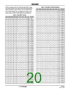
TABLE 3. PHASE DROPPING CONFIGURATION AT PSI1 AND
PSI2/3/DECAY
PSI2/3
SICI NPSI CODE
PSI1 Mode
1-Phase
2-Phase
1-Phase
2-Phase
& DECAY
1-Phase
1-Phase
1-Phase
1-Phase
0
0
1
1
0
1
0
1
SI1
SI2
CI1
CI2
SI, (N-1)-CI
SI, (N-2)-CI
2-Phase CI
2-Phase CI
SWITCHING FREQUENCY (Hz)
FIGURE 4. SWITCHING FREQUENCY vs RT
NOTE: For 2-Phase CI option, the dropped coupled phase turns on LGATE
to circulate current when PWM1 is high.
FN6964.0
January 3, 2011
16

 INTERSIL [ Intersil ]