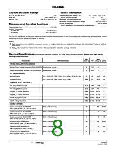
ISL6366
resistor value can be effectively set at 60Ω to 1.8kΩ. When VR0
is disabled (PWM1 = VCC), connect 1MΩ from this pin to GND.
pin or keeping it open virtually disables this feature. If the droop
option of VR1 is disabled, then this pin becomes DVCS. A series
resistor and capacitor can be connected from this pin to the FBS
pin to compensate and smooth dynamic VID transitions for VR1
output.
ISENS+, ISENS - The ISENS+ and ISENS- pins are current sense
inputs to the differential amplifier of VR1. The sensed current is
used for overcurrent protection and droop regulation. For DCR
sensing, connect each ISENS- pin to the node between the RC
sense elements. Tie the ISENS+ pin to the other end of the sense
FSS_DRPS - A resistor placed from this pin to ground/VCC will set
the switching frequency of VR1. The relationship between the
value of the resistor and the switching frequency will be
capacitor through a resistor, R
. The voltage across the
ISENS
sense capacitor is proportional to the inductor current. Therefore,
the sense current is proportional to the inductor current and
approximated by Equation 4 on page 16. This pin is also used to
set the droop option. The droop is disabled when the resistor is
pulled to VCC and enabled when the resistor is pulled to ground.
When VR1 is disabled (PWMS = VCC), connect 1MΩ from this pin
to GND for ADDR: 0, 2, 4, and 6; to VCC for ADDR: 8, A, and C.
scaled by the DCR of the inductor and R
. When VR1 is
ISENS
disabled, have ISENS- grounded and ISENS+ open.
IMON - IMON is the output pin of sensed, thermally compensated (if
internal thermal compensation is used) average current of VR0. The
voltage at the IMON pin is proportional to the load current and the
resistor value, and internally clamped to 1.12V. If the clamped
voltage is triggered, it will initiate an overcurrent shutdown. By
choosing the proper value for the resistor at IMON pin, the
overcurrent trip level can be set to be lower than the fixed internal
overcurrent threshold. During the dynamic VID, the OCP function of
this pin is disabled to avoid false triggering. Tie it to GND if not used.
Does not need to refer to the remote ground for VR12/IMPV7
applications.
TMS - This is an input pin for the temperature monitoring. Connect
this pin through an NTC thermistor to GND and a resistor to VCC of
the controller. The voltage at this pin is inversely proportional to
the VR temperature. The thermal information can be used for VR1
thermal compensation. If TCOMPS is set at “OFF” bit, the
integrated thermal compensation is disabled; otherwise, the
thermal information is used for VR1 thermal compensation with
“TCOMPS” data. Combined with TM pin, the thermal information at
TMS pin will also be used to trigger VR_HOT#. The NTC should be
placed close to the current sensing element, the output inductor or
dedicated sense resistor of VR1. If not used, connect this pin to TM
or 1MΩ/2MΩ resistor divider, but DON’T tie it to VCC or GND.
FS_DRP - A resistor placed from this pin to GND/VCC will set the
switching frequency of VR0. The relationship between the value
of the resistor and the switching frequency will be approximated
by Equation 4 on page 16. This pin is also used to set the droop
option. The droop is disabled when the resistor is pulled to VCC
and enabled when the resistor is pulled to ground. When VR0 is
disabled (PWM1 = VCC), connect 1MΩ from this pin to GND.
SVCLK - An input pin for a synchronous clock signal of SerialVID
bus from CPU.
SVDATA - An input pin for transferring open-drain data signals
between CPU and VR controller.
SVALERT# - An output pin for transferring the active low signal
driven asynchronously from the VR controller to CPU.
HFCOMP - Connect a resistor with a similar value of the feedback
impedance to the VR0 output to compensate the level-shifted
output voltage during high-frequency load transient events.
Connecting more than 2x of feedback impedance to this pin or
keeping it open virtually disables this feature.
RAMP_ADJ - An input pin to set the slope of Sawtooth for VR0.
The slope of the Sawtooth is proportional to the current, sampled
by the an active pull-down device, into this pin. When the resistor
is connected to the input voltage of the VR0, the slope will be
proportional to the input voltage, achieving voltage feed-forward
PSICOMP - Connect an RC to the type III compensation capacitor
of the VR0 output voltage. This improves loop gain and load
transient response in PSI1/2/3/Decay mode. An open pin will
disable this feature.
compensation. For a 12V supply (V ) and 2.4MΩ pull up (~ 5µA),
IN
it sets a nominal 0.25V/µs up-ramp slope at 500kHz switching
frequency, corresponding to 0.5V peak-to-peak up ramp. The
maximum peak-to-peak up ramp should be limited to 3V,
corresponding a pull-down current of 30µA at 500kHz, i.e., the
SICI - When this pin is pulled to ground, it sets for standard inductor
(SI) operation; when this pin is pulled to VCC, it sets coupled-inductor
(CI) operation. The phase dropping operation options for PSI1/2/3
mode are summarized in Table 3 on page 16.
pull-up impedance should be higher than V /30µA at 500kHz.
IN
See Equation 3 for the up ramp amplitude calculation. When this
pin is floating, the up ramp amplitude sets to 1V regardless of
the switching frequency and the feedforward function is
disabled.
DVC - A series resistor and capacitor can be connected from this
pin to the FB pin to compensate and smooth dynamic VID
transitions.
ADDR_IMAXS_TMAX, BTS_DES_TCOMPS, BT_FDVID_TCOMP,
NSPI_DE_IMAX - These are four register pins to program system
parameters. The meaning of each is described as below. See
Table 9 for the summary.
VSENS, RGNDS, FBS, COMPS, VR_RDYS, IMONS, FSS_DRPS,
HFCOMPS - These pins are for VR1 regulator and have the same
function as VSEN, RGND, FB, COMP, VR_RDY, IMON, FS_DRP, and
HFCOMP, respectively. However, HFCOMPS has multiplexed the
DVCS function, while the FSS_DRPS does have additional
programming feature as described in the following.
ADDR_IMAXS_TMAX (0C):
ADDR - An input pin to set the address offset register of VR0 (0,
2, 4, 6, 8, A, C) and VR1 (1, 3, 5, 7). E/F is an ALL call address
and is not used.
HFCOMPS/DVCS - Connect a resistor with a similar value of the
feedback impedance to the VR1 output to compensate the level-
shifted output voltage during high-frequency load transient
events. Connecting more than 2x of feedback impedance to this
FN6964.0
January 3, 2011
12

 INTERSIL [ Intersil ]