ISL6366
L/DCR OR ESL/R
MATCHING
Channel-Current Balance for VR0
SEN
Assuming the compensator design is correct, Figure 11 shows the
expected load transient response waveforms if L/DCR or
The sensed current I from each active channel is summed
together and divided by the number of active channels. The
n
ESL/R
current I
OUT
is matching the R-C time constant. When the load
has a square change, the output voltage V also
resulting average current I
provides a measure of the total
SEN
AVG
load current. Channel current balance is achieved by comparing
the sensed current of each channel to the average current to
make an appropriate adjustment to the PWM duty cycle of each
channel with Intersil’s patented current-balance method.
OUT
has a square response, except for the overshoot at load release.
However, there is always some PCB contact impedance of current
sensing components between the two current sensing points; it
hardly accounts into the L/DCR or ESL/R
matching calculation.
SEN
Channel current balance is essential in achieving the thermal
advantage of multiphase operation. With good current balance,
the power loss is equally dissipated over multiple devices and a
greater area.
Fine tuning the matching is necessarily done in the board level to
improve overall transient performance and system reliability.
If the R-C timing constant is too large or too small, V (s) will not
C
accurately represent real-time I
(s) and will worsen the
OUT
transient response. Figure 12 shows the load transient response
when the R-C timing constant is too small. V will sag
excessively upon load insertion and may create a system failure
or early overcurrent trip. Figure 13 shows the transient response
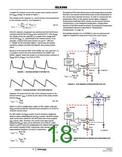
Voltage Regulation
OUT
The compensation network shown in Figure 14 assures that the
steady-state error in the output voltage is limited only to the error
in the reference voltage (DAC & OFFSET) and droop current
source, remote sense, and error amplifier.
when the R-C timing constant is too large. V
is sluggish in
OUT
drooping to its final value. There will be excessive overshoot if
load insertion occurs during this time, which may potentially hurt
the CPU reliability.
The sensed average current I
DROOP
is tied to FB internally and
will develop voltage drop across the resistor between FB and
for droop control. This current can be disconnected from the
V
OUT
FB node by tying R
IOUT
high to VCC for non-droop applications.
FS_DRP
The output of the error amplifier, V , is compared to the internal
COMP
sawtooth waveforms to generate the PWM signals. The PWM
signals control the timing of the Intersil MOSFET drivers and regulate
the converter output to the specified reference voltage.
VOUT
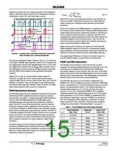
FIGURE 11. DESIRED LOAD TRANSIENT RESPONSE
WAVEFORMS
The ISL6366 does not have a unity gain amplifier in between the
feedback path and error amplifier. For remote sensing, connect the
microprocessor sensing pins to the non-inverting input, FB, via the
feedback resistor (R ), and inverting input, RGND, of the error
FB
amplifier. This configuration effectively removes the voltage error
encountered when measuring the output voltage relative to the local
controller ground reference point. VSEN should connect to remote
sensing’s positive rail as well for over voltage protection.
IOUT
VOUT
EXTERNAL CIRCUIT
ISL6366
R
C
C
C
COMP
I
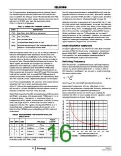
FIGURE 12. LOAD TRANSIENT RESPONSE WHEN R-C TIME
CONSTANT IS TOO SMALL
DROOP
ERROR
AMPLIFIER
FB
-
IOUT
RGND
+
V
+
COMP
+
VID &
OFFSET
+
V
-
DAC
VOUT
R
FB
DROOP
-
VSEN
OVP
+
-
+
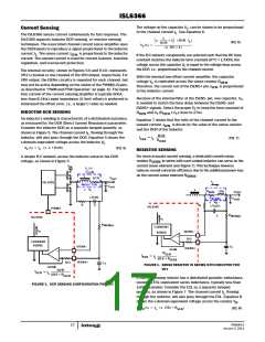
FIGURE 13. LOAD TRANSIENT RESPONSE WHEN R-C TIME
CONSTANT IS TOO LARGE
V
OUT
FIGURE 14. OUTPUT VOLTAGE AND LOAD-LINE REGULATION
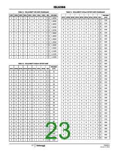
A digital-to-analog converter (DAC) generates a reference voltage,
which is programmable via SVID bus. The DAC decodes the SVID
set command into one of the discrete voltages shown in Table 4.
In addition, the output voltage can be margined in ±5mV step
between -640mV and 635mV, as shown in Table 5, via SVID set
FN6964.0
January 3, 2011
19

 INTERSIL [ Intersil ]