ISL6366
logic output. When OCP or OVP occurs in VR0, VR_RDY will be
pulled to low.
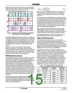
Functional Pin Descriptions
Note: VR0 is the multi-phase voltage regulator. VR1 is the
single-phase voltage regulator. Refer to Table 13 on page 35 and
Table 14 on page 39 for Design and Layout Consideration.
TM - TM is an input pin for the VR0 temperature measurement.
Connect this pin through an NTC thermistor to GND and a resistor
to VCC of the controller. The voltage at this pin is inversely
proportional to the VR temperature. The device monitors the VR
temperature based on the voltage at the TM pin. Combining with
“TCOMP” setting, VR0’s sensed current is thermally compensated.
The VR_HOT# asserts low if the sensed temperature at this pin is
higher than the maximum desired temperature, “TMAX”. The NTC
should be placed close to the current sensing element, the output
inductor or dedicated sense resistor on Phase 1 of VR0. A
decoupling capacitor (0.1µF) is typically needed to be in close
proximity to the controller. If not used, connect this pin to TMS or
1MΩ/2MΩ resistor divider, but DON’T tie it to VCC or GND.
VCC - Supplies the power necessary to operate the chip. The
controller starts to operate when the voltage on this pin exceeds
the rising POR threshold and shuts down when the voltage on
this pin drops below the falling POR threshold. Connect this pin
directly to a +5V supply with a high quality ceramic capacitor.
GND - The bottom metal base of ISL6366 is the GND. Bias and
reference ground for the IC. It is also the return for all PWM
output drivers.
EN_PWR - This pin is a threshold-sensitive enable input.
Connecting the power train input supply to this through an
appropriate resistor divider provides a means to synchronize the
power sequencing of the controller and the MOSFET driver ICs.
When EN_PWR is driven above 0.85V, the ISL6366 is actively
depending on status of the EN_VTT, the internal POR, and
pending fault states. Driving EN_PWR below 0.75V will clear all
fault states and prepare the ISL6366 to soft-start when re-
enabled.
VR_HOT# - VR_HOT# is used as an indication of high VR
temperature. It is an open-drain logic output. It will be open if the
measured VR temperature is less than a certain level, and pulled
low when the measured VR temperature reaches a certain level.
PWM[6:1] - Pulse width modulation outputs of VR0. Connect
these pins to the PWM input pins of the Intersil driver IC. The
number of active channels is determined by the state of
PWM[6:2]. Tie PWM(N+1) to VCC to configure for N-phase
operation. PWM firing order is sequential from 1 to N with N
being the number of active phases. If PWM1 is tied high, the
respective address is released for use, i.e, the VR0 is disabled
and does not respond to the SVID commands. IMON, VSEN, FB,
ISEN[6:1]-, and RGND must be grounded to remove OCP and OVP
faults of VR0, while TM can be tied to TMS, or 1/2 ratio resistor
divider. In addition, must connect FS_DRP to 1MΩ from GND or
VCC. See Table 1 on page 15 and Table 13 on page 35 for details.
EN_VTT - This pin is a threshold-sensitive enable input. It’s
typically connected to the output of the VTT voltage regulator in
the computer mother board. When this pin is driven above 0.85V,
the ISL6366 is actively depending on status of the EN_PWR, the
internal POR, and pending fault states. Driving this below 0.75V
will clear all fault states and prepare the ISL6366 to soft-start
when re-enabled.
VSEN - This pin monitors the regulator VR0 output for over-
voltage protection. Connect this pin to the positive rail remote
sensing point of the microprocessor or load. This pin tracks with
the FB pin. If a resistive divider is placed on the FB pin, a resistive
divider with the same ratio should be on the VSEN pin. Tie it to
GND if not used.
PWMS - Pulse width modulation output of VR1. Connect this pin
to the PWM input pin of the Intersil driver IC. Tie this pin to VCC to
disable this PWM channel, while the respective address is
released for use, i.e., the VR1 is disabled and does not respond to
the SVID commands. IMONS, VSENS, FBS, ISENS-, and RGNDS
must be grounded to remove OCP and OVP faults of VR1, while
TMS can be tied to TM, or 1/2 ratio resistor divider. In addition,
must connect FSS_DRPS to 1MΩ from GND or VCC for proper
SVID address. See Table 13 on page 35 for details.
RGND - This pin compensates the offset between the remote
ground of the VR0 load and the local ground of this device.
Connect this pin to the negative rail remote sensing point of the
microprocessor or load. Tie it to GND if not used.
COMP and FB - COMP and FB are the output and inverting input
of the precision error amplifier, respectively. A type III loop
compensation network should be connected to these pins, while
the FB’s R-C network should connect to the positive rail remote
sensing point of the microprocessor or load. Combined with
RGND, the potential difference between remote and local rails is
completely compensated and it improves regulation accuracy. A
properly chosen resistor between FB and remote sensing point
can set the load line (droop, if enabled), because the sensed
current will flow out of FB pin. The droop scale factor is set by the
ratio of the effective ISEN resistors (set by RSET) and the inductor
DCR or the dedicated current sense resistor. COMP is tied back to
FB through an external R-C network to compensate the regulator.
An RC from the FB pin to ground will be needed if the output is
lagging from the DAC, typically for applications with too many
output capacitors and droop enabled.
ISEN[6:1]+, ISEN[6:1] - The ISEN+ and ISEN- pins are current
sense inputs to individual differential amplifiers of VR0. The
sensed current is used for channel current balancing, overcurrent
protection, and droop regulation. Inactive channels should have
their respective current sense inputs, ISEN[6:#]- grounded, and
ISEN[6:#]+ open. For example, ground ISEN[6:5]- and open
ISEN[6:5]+ for 4-phase operation. DON’T ground ISEN[6:1]+. For
DCR sensing, connect each ISEN- pin to the node between the RC
sense elements. Tie the ISEN+ pin to the other end of the sense
capacitor (typically output rail). The voltage across the sense
capacitor is proportional to the inductor current. Therefore, the
sensed current is proportional to the inductor current and scaled
by the DCR of the inductor and R . When VR0 is disabled, have
SET
ISEN[6:1]- grounded and ISEN[6:1]+ open.
RSET - A resistor connected from this pin to ground sets the
current gain of the current sensing amplifier for VR0. The RSET
resistor value can be from 3.84kΩ to 115.2kΩ and is 64x of the
VR_RDY - VR_RDY indicates that soft-start has completed and
this VR0 output remains in normal operation. It is an open-drain
required R
resistor value. Therefore, the current sense gain
ISEN
FN6964.0
January 3, 2011
11

 INTERSIL [ Intersil ]